Preprocessing device for chip detection

A preprocessing device and chip detection technology, applied in the direction of measuring device, test sample preparation, sampling, etc., can solve the problems of twisting and bowing value deviation, uneven height of scraped solder balls, chip scratches, etc., to achieve The effect of uniform height, simple structure and fast eradication

Pending Publication Date: 2019-12-13
CHIPMOS TECHSHANGHAI
View PDF0 Cites 0 Cited by
  • Summary
  • Abstract
  • Description
  • Claims
  • Application Information

AI Technical Summary

Problems solved by technology

[0004] The inventors of the present application have found that due to the chip products of BAG (Ball Grid Array Package) in the prior art, there are protruding solder balls on the chip substrate on one side, which will be affected by the height of the solder balls, which will cause the chip to be tested. The twist and bow values ​​deviate, so it is necessary to remove the solder balls on the chip substrate before accurately testing the chip
In the existing production, the solder balls on the chip substrate are generally removed by manual scraping with a blade. There are problems of uneven height and low efficiency of scraping the solder balls, and there is a risk of the chip being scratched

Method used


Image

  • Preprocessing device for chip detection
  • Preprocessing device for chip detection
  • Preprocessing device for chip detection

Examples


Embodiment Construction

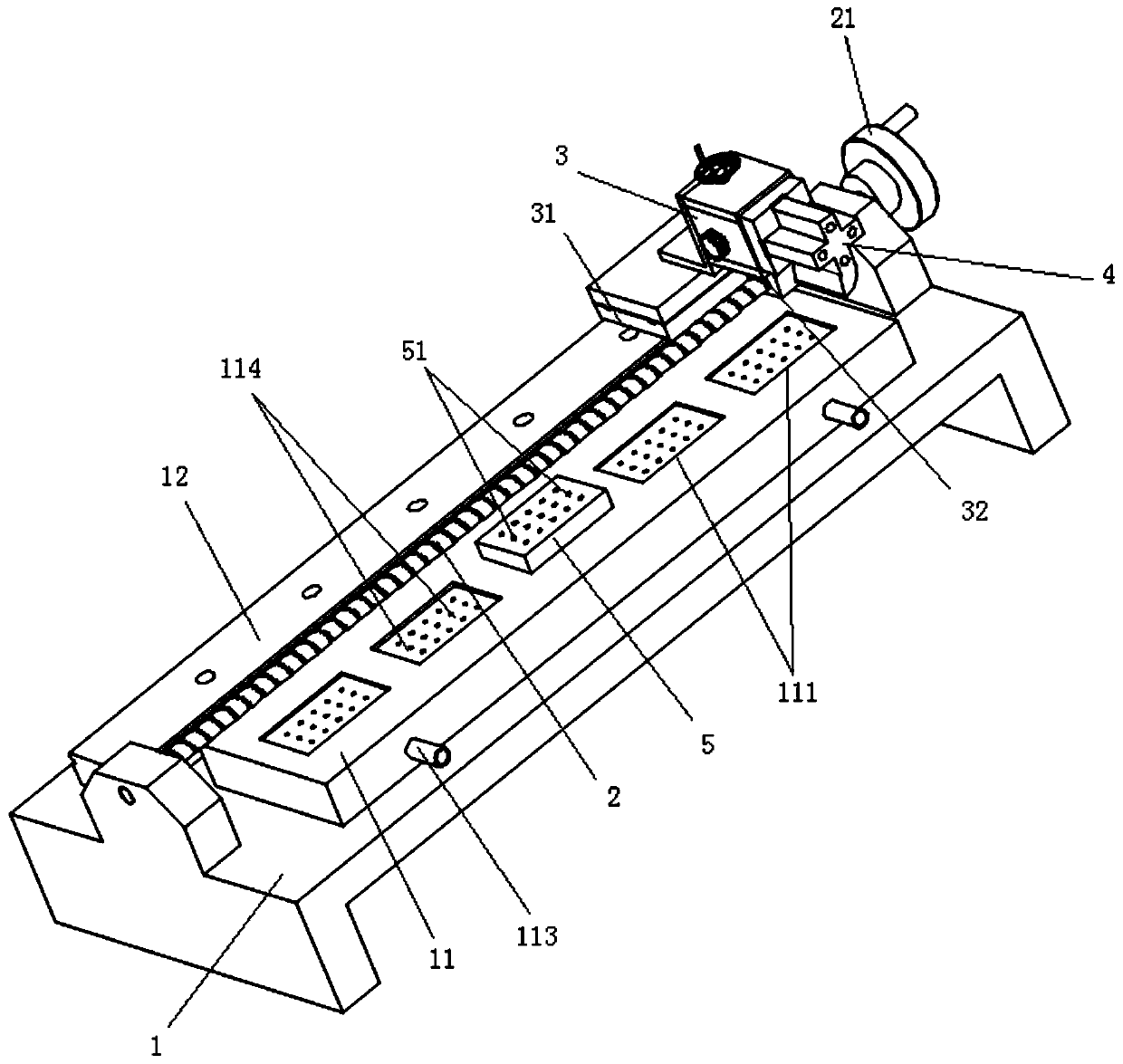
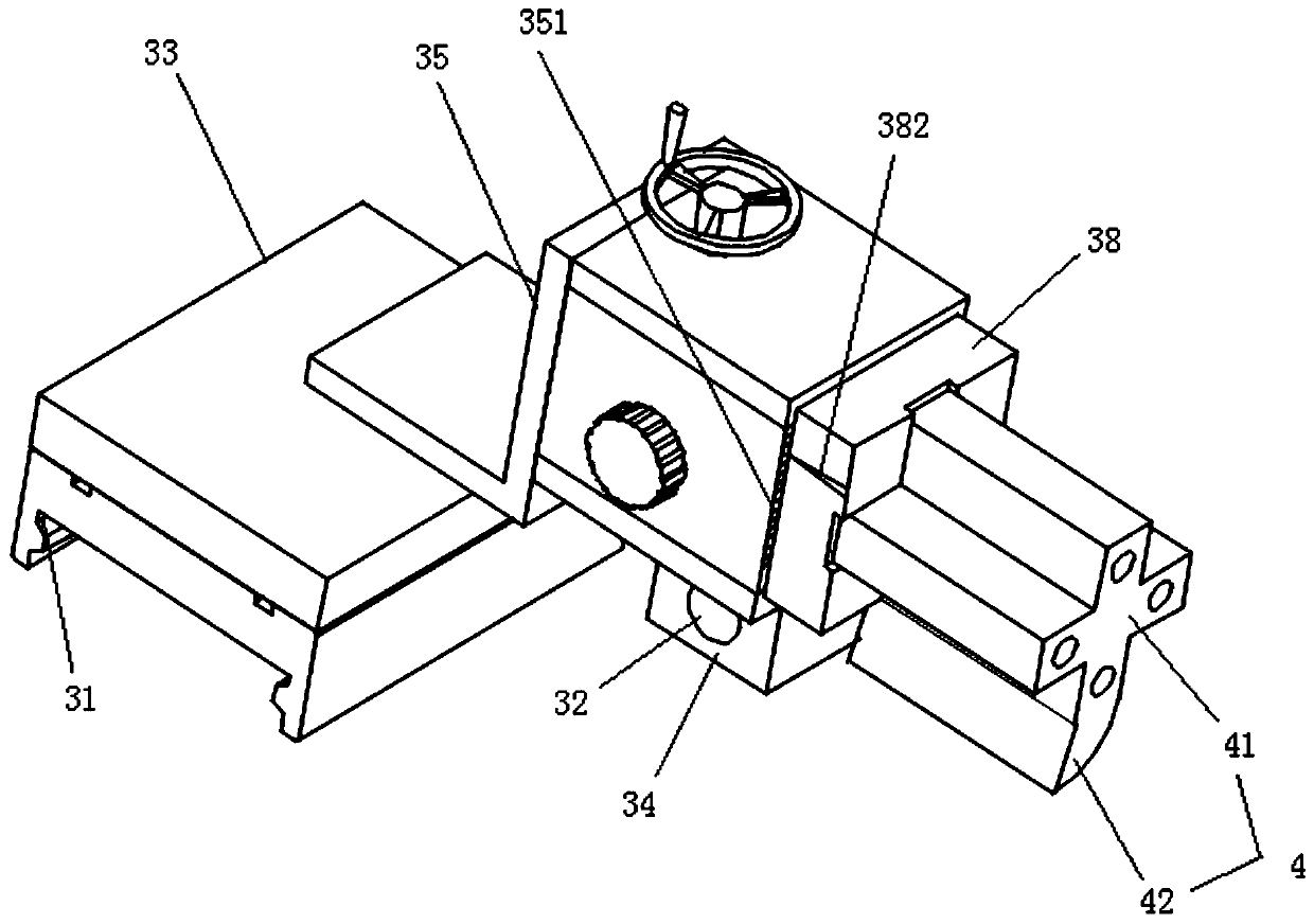
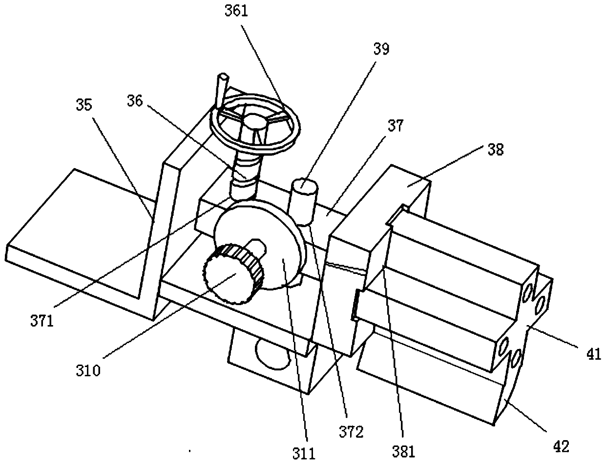
[0050] In order to make the objectives, technical solutions, and advantages of the embodiments of the present invention clearer, the technical solutions in the embodiments of the present invention will be described clearly and completely in conjunction with the accompanying drawings in the embodiments of the present invention. Obviously, the described embodiments It is a part of the embodiments of the present invention, not all the embodiments. Based on the embodiments of the present invention, all other embodiments obtained by those of ordinary skill in the art without creative work shall fall within the protection scope of the present invention.

[0051] In the description of the present invention, it should be understood that the terms "center", "longitudinal", "transverse", "upper", "lower", "front", "rear", "left", "right", " The orientation or positional relationship indicated by "vertical", "horizontal", "top", "bottom", "inner", "outer", "axial", "radial", and "circumfere...


PUM


Abstract

The embodiment of the invention discloses a preprocessing device for chip detection. The device comprises a supporting table, a first lead screw, a tool apron and a push broach; a base is arranged onthe supporting table, and a rectangular groove for containing a chip is formed in the base; a first sliding rail is arranged on the supporting table, and the first lead screw is rotatably arranged onthe supporting table; a push broach is arranged on the tool apron, and the tool apron is slidably arranged on the first sliding rail on the supporting table, and the tool apron is meshed with the first lead screw. According to the invention, the first lead screw rotates to drive the tool apron and the push broach to slide along the first sliding rail, and the push broach shovels solder balls placed on a chip substrate in the rectangular groove of the base when sliding. The device is simple in structure and convenient to use, the shoveled solder balls are uniform in height, and the accuracy ofsubsequent detection of distortion and bow values of the chip is guaranteed.

Description

Technical field [0001] The embodiment of the present invention relates to the field of chip technology, in particular to a pre-processing device for chip detection. Background technique [0002] With the advancement of integration technology, the improvement of equipment and the use of deep sub-micron technology, the integration of silicon single-chips has continued to increase, the number of I / O pins has increased sharply, and the power consumption has also increased. The packaging requirements for integrated circuits have become more strict. In order to meet the development needs of integrated circuits, on the basis of the original packaging varieties, a new packaging method-ball grid array packaging, referred to as BAG (Ball Grid Array Package), is added. [0003] BAG (Ball Grid Array Package) chip products are cube-shaped. After the chip is packaged, a thermal distortion test is required to detect the distortion and bow of the chip. The projection moire technology (Shadow Moi...

Claims


Application Information

Patent Timeline
Patent Type & Authority Applications(China)
IPC IPC(8): G01N1/28
CPCG01N1/286
Inventor 施明张健健王晓穆连芳
Owner CHIPMOS TECHSHANGHAI
Why Eureka
Try Eureka