Terahertz metamaterial biosensor and its preparation method and detection method
A technology of biosensors and metamaterials, applied in the fields of analyzing materials, analyzing materials through optical means, instruments, etc., can solve problems such as time-consuming, complicated operation, and inability to meet rapid detection
- Summary
- Abstract
- Description
- Claims
- Application Information
AI Technical Summary
Problems solved by technology
Method used
Image
Examples
preparation example Construction
[0084] The metal preparation method is as follows: the growth method of the bottom metal layer is electroplating or magnetron sputtering, and the growth method of the surface layer gold is electron beam evaporation.
[0085] In some embodiments of the present invention, the response waveband of the biosensor is in the terahertz range, and the waveband range is 0.5-3THz.
[0086] In some embodiments of the present invention, the antibodies or probes modified on the metamaterial to recognize different cancer markers are: CEA (carcinoembryonic antigen), CA125 (glycoprotein antigen 125), AFP (alpha-fetoprotein) , CA15-3 (glycoprotein antigen 15-3), GGT-II (glutamyl transpeptidase isozyme II), CA19-9 (glycoprotein antigen 19-9), CA42 (glycoprotein antigen 42), microRNA4484 , microRNA3646 and other conventional cancer marker antibodies and microRNA probes.
[0087] As mentioned above, the detection method of the negative refractive index terahertz metamaterial biosensor for early w...
Embodiment 1
[0133] The negative refractive index terahertz metamaterial biosensor was prepared according to the following steps:
[0134] (1) Substrate preparation: Boil in acetone solution for 8 minutes to remove organic pollutants on the substrate surface before performing metamaterial processing, then boil in absolute ethanol solution for 10 minutes to remove acetone, and finally rinse with deionized water for three Blow dry with nitrogen.
[0135] (2) Metamaterial structure construction:
[0136] The transfer of the metamaterial pattern on the substrate is realized by micro-nano-fabrication lithography technology. First, a photoresist (AR-N4340) was coated on the previously processed substrate by spin coating. Prebake at 95°C for 15 minutes, exposure to build those metamaterial structures on the substrate, and postbake at 105°C for 10 minutes.
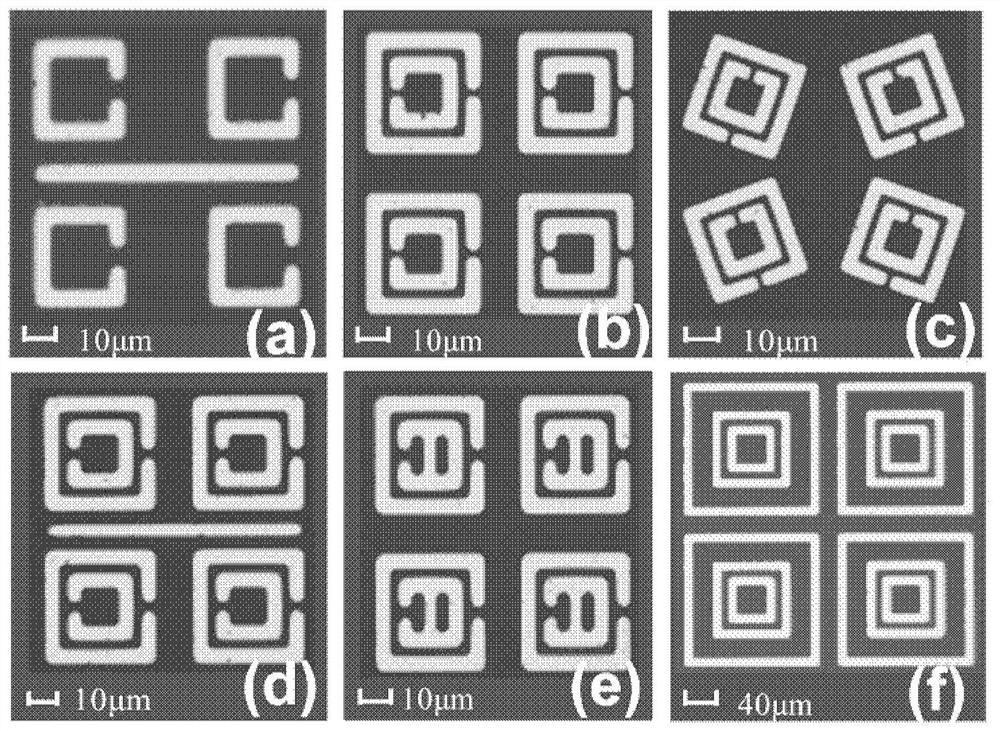
[0137] The prepared metamaterial structure is a rotating double ring structure, the metamaterial pattern is a rotating double split ring, ...
Embodiment 2
[0146] This embodiment is basically the same as Embodiment 1, the difference is:
[0147] In step (4), the substrate is a 300 μm silicon substrate, which is thinned to 150 μm by a substrate thinning process. After the thinning process, it should be boiled in acetone solution for 10 minutes to remove organic pollutants on the substrate surface, then boiled in absolute ethanol solution for 15 minutes to remove acetone, finally rinsed with deionized water three times, and dried with nitrogen.
PUM
| Property | Measurement | Unit |
|---|---|---|
| thickness | aaaaa | aaaaa |
| thickness | aaaaa | aaaaa |
| thickness | aaaaa | aaaaa |
Abstract
Description
Claims
Application Information


