Wafer etching device

A technology for etching equipment and wafers, used in electrical components, semiconductor/solid-state device manufacturing, circuits, etc., to solve the problems of etching liquid flow, difficult control, and different widths at different heights of etching positions, so as to reduce the difference. , reduce the residence time, avoid the effect of flowing around

Active Publication Date: 2019-12-31
深圳市中科光芯半导体科技有限公司
View PDF9 Cites 0 Cited by
  • Summary
  • Abstract
  • Description
  • Claims
  • Application Information

AI Technical Summary

Problems solved by technology

[0003] Because the etchant stays on the wafer during etching, the etchant will flow around, which is difficult to control. The longer the stay time, the more the etchant flows, which will lead to different widths at different heights of the etched position, resulting in difference

Method used


Image

  • Wafer etching device
  • Wafer etching device
  • Wafer etching device

Examples


Embodiment Construction

[0025] The following will clearly and completely describe the technical solutions in the embodiments of the present invention with reference to the accompanying drawings in the embodiments of the present invention. Obviously, the described embodiments are only some, not all, embodiments of the present invention. Based on the embodiments of the present invention, all other embodiments obtained by persons of ordinary skill in the art without making creative efforts belong to the protection scope of the present invention.

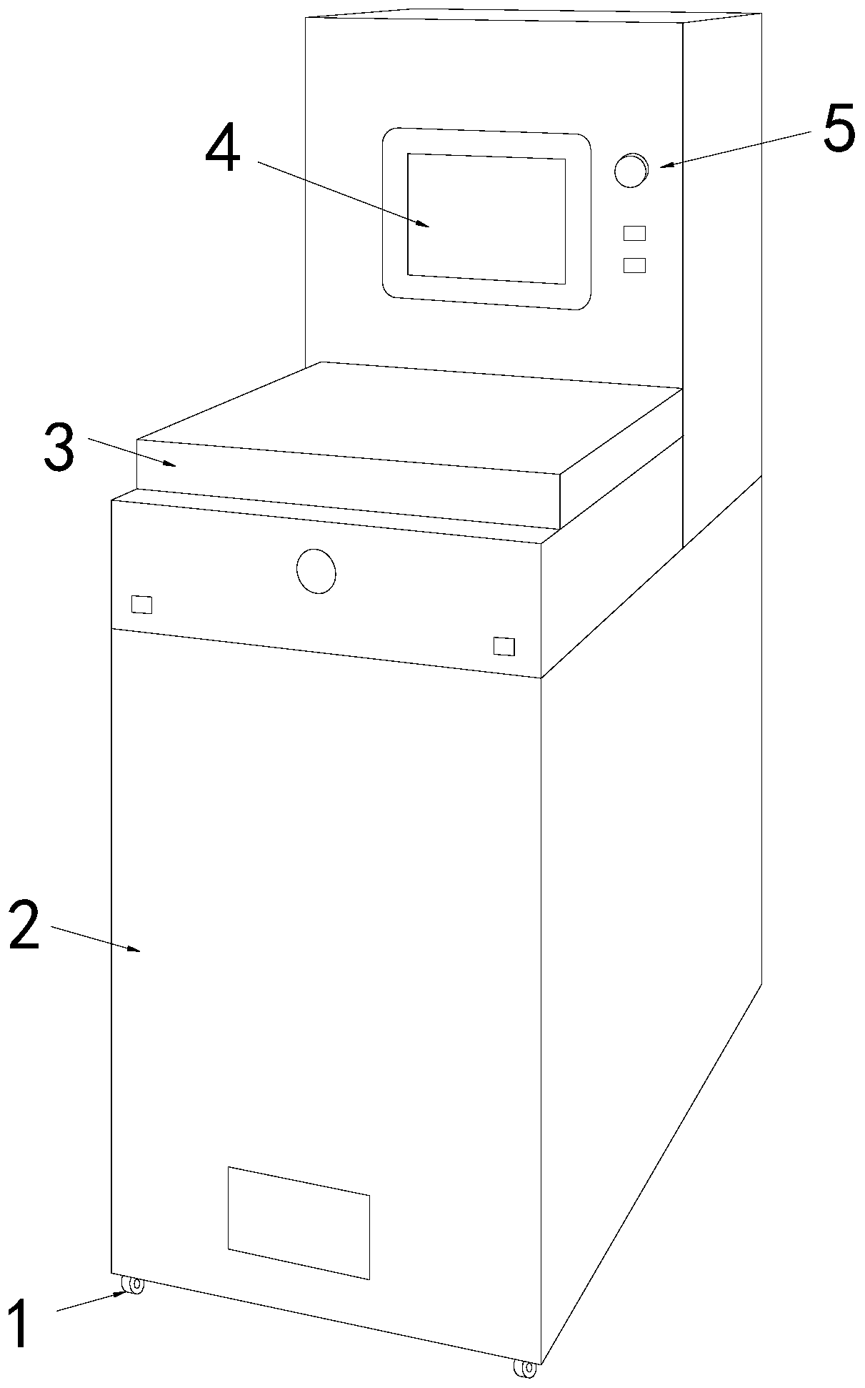
[0026] see Figure 1-4 , the present invention provides a technical solution for wafer etching equipment: its structure includes a moving wheel 1, an etching box 2, a box cover 3, a display screen 4, and a control box 5, and the bottom of the etching box 2 is equipped with a moving wheel 1 , the top of the etching box 2 is provided with a box cover 3, the control box 5 is located on the side of the box cover 3 and connected to the top of the etching box 2, the...


PUM


Abstract

The invention discloses a wafer etching device. The structure comprises moving wheels, an etching box, a box cover, a display screen and a control box. The moving wheels are arranged at the bottom ofthe etching box. The box cover is arranged at the top of the etching box. The control box is arranged on the side of the box cover and connected with the top of the etching box. The display screen isarranged on the surface of the control box. A stage, a first clamp, a second clamp, an ejector, a cylinder, a Y axis guide rail and an X axis guide rail are arranged in the etching box. The stage is connected with the bottom of the box cover. The first and second clamps are arranged on two sides of the bottom of the stage. The ejector is located below the stage. The bottom of the ejector is connected with the cylinder. The cylinder is arranged on the Y axis guide rail. The wafer etching device provided by the invention has the advantages that a series of rapid operations of spraying and sucking back can reduce the residence time of an etchant and prevent the etchant from flowing around; the etchant can be ejected from the bottom to the top, which can reduce the probability of flowing around of the etchant, and enables the etchant to flow downward; and the difference in the height of etching positions can be reduced.

Description

technical field [0001] The invention relates to the field of wafers, in particular to wafer etching equipment. Background technique [0002] Wafers are the basic raw materials for manufacturing semiconductor devices, and are used in the processing of thin film circuits, printed circuits and other fine graphics. [0003] Because the etchant stays on the wafer during etching, the etchant will flow around, which is difficult to control. The longer the stay time, the more the etchant flows, which will lead to different widths at different heights of the etched position, resulting in difference. Contents of the invention [0004] The main purpose of the present invention is to overcome the deficiencies of the prior art and provide a wafer etching equipment. [0005] The present invention adopts the following technical solutions to achieve: a wafer etching equipment, the structure of which includes a moving wheel, an etching box, a box cover, a display screen, and a control bo...

Claims


Application Information

Patent Timeline
Patent Type & Authority Applications(China)
IPC IPC(8): H01L21/67
CPCH01L21/6708
Inventor 汪洪安
Owner 深圳市中科光芯半导体科技有限公司
Why Eureka
Try Eureka