Unlock instant, AI-driven research and patent intelligence for your innovation.

Array substrate and oled display panel

A technology for array substrates and display panels, which is applied to semiconductor devices, electrical components, circuits, etc., can solve the problems of different luminous brightness and uneven display brightness of OLED display panels, and achieve the effect of reducing brightness differences and improving brightness uniformity

Active Publication Date: 2022-06-03
KUNSHAN GO VISIONOX OPTO ELECTRONICS CO LTD
View PDF11 Cites 0 Cited by
  • Summary
  • Abstract
  • Description
  • Claims
  • Application Information

AI Technical Summary

Problems solved by technology

However, when the OLED display panel is displaying, there will be a resistance voltage drop in the wire. The resistance voltage drop is caused by the resistance voltage division of the wire in the OLED display panel itself, that is, when the current passes through the wire in the display panel, the wire will generate With a certain voltage drop, the pixel units located at different positions are affected by the voltage drop, resulting in different luminous brightness of each pixel unit, resulting in uneven display brightness of the OLED display panel.

Method used


Image

  • Array substrate and oled display panel
  • Array substrate and oled display panel
  • Array substrate and oled display panel

Examples


Embodiment Construction

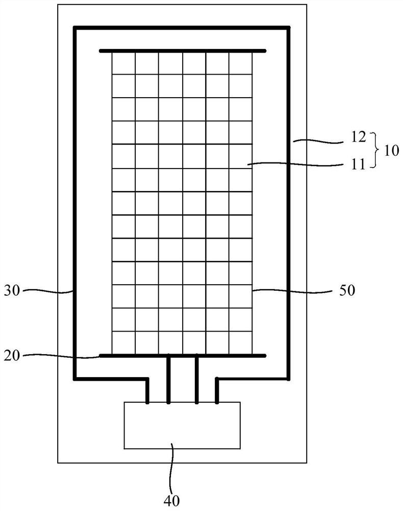
[0036] As shown in FIG. 1, in the existing organic electroluminescent diode (OLED) display panel, through the signal wiring to the image

[0038] However, due to the resistance of the VDD signal line 50 itself, the VDD power supply signal is close to the driver chip on the VDD signal line 50

[0039] As shown in FIG. 2, in order to solve the above problems, the array substrate provided by the embodiment of the present invention includes a substrate 10 and a device

[0041] The non-display area 12 is used for arranging various metal traces, which can provide operating voltage and

[0045] Since the first signal line 51 and the second signal line 52 themselves have a voltage drop, the first signal line 51 along the first power supply line 21

[0046] In this embodiment, the first signal line 51 and the second signal line 52 are alternately arranged in the display area 11, and can be located in different positions.

[0047] In this embodiment, the driving chip 40 and the first power s...


PUM


Abstract

The invention provides an array substrate and an OLED display panel, which belong to the field of display technology. The array substrate includes a substrate and a first power supply line and a second power supply line arranged on the substrate; the first power supply line Set opposite to the second power supply line, a plurality of first signal lines and a plurality of second signal lines are alternately arranged between the first power supply line and the second power supply line; each first signal line is connected to a plurality of pixel units , and one end of each first signal line is connected to the first power supply line, and the other end is grounded; each second signal line is connected to a plurality of pixel units, and one end of each second signal line is connected to the second The power supply wire is connected, and the other end is grounded. The array substrate and the display panel provided by the invention reduce the brightness difference of the display panel and improve the brightness uniformity of the display panel.

Description

Array substrate and OLED display panel technical field [0001] The present invention relates to the field of display technology, and in particular, to an array substrate and an OLED display panel. Background technique In the field of display, organic electroluminescent diode (Organic Light-Emitting Diode, referred to as OLED) display panel has the characteristics of self-luminescence, high contrast ratio, low energy consumption, wide viewing angle, fast response speed and simple manufacturing. There are broad prospects for development. [0003] The OLED display panel includes a plurality of pixel units arranged in an array, and each pixel unit in the same column passes through a The wires are connected, and each pixel unit in the same column can be displayed by applying a voltage to the wires. However, when OLED displays When the display panel is displaying, there will be a resistance voltage drop in the wires. The resistance voltage drop is due to the wires themselv...

Claims


Application Information

Patent Timeline
Patent Type & Authority Patents(China)
IPC IPC(8): H01L27/32
CPCH10K59/10H10K59/131
Inventor 齐栋宇韩珍珍胡思明吴剑龙
Owner KUNSHAN GO VISIONOX OPTO ELECTRONICS CO LTD