Display device

A technology for display devices and display areas, which is applied in the directions of identification devices, nonlinear optics, instruments, etc., can solve problems such as not being able to go directly to the back of the hole (away from the side of the backlight, affecting display effects, brightness differences, etc., to achieve Improve display effects and user experience, improve display uniformity, and eliminate brightness differences

Active Publication Date: 2018-12-04
XIAMEN TIANMA MICRO ELECTRONICS
View PDF3 Cites 17 Cited by
  • Summary
  • Abstract
  • Description
  • Claims
  • Application Information

AI Technical Summary

Problems solved by technology

In the prior art, based on the structural design of the full screen, holes need to be drilled in the display area of ​​the panel to install cameras, earpieces, sensors, etc. Hole, the light cannot go directly to the back of the hole (away from the backlight side), so that the light cannot reach the back area of ​​the hole, and dark areas and shadows will appear at the back of the hole, so the front of the hole (closer to the backlight source side) will be brighter than the back of the hole, and as the size of the hole gets larger, the difference in brightness between the front of the hole and the back of the hole gets bigger
[0003] To sum up, the side-type backlight full-screen display products in the prior art have differences in the brightness of the area around the hole-digging area, resulting in uneven display brightness and affecting the display effect.

Method used


Image

  • Display device
  • Display device
  • Display device

Examples


Embodiment Construction

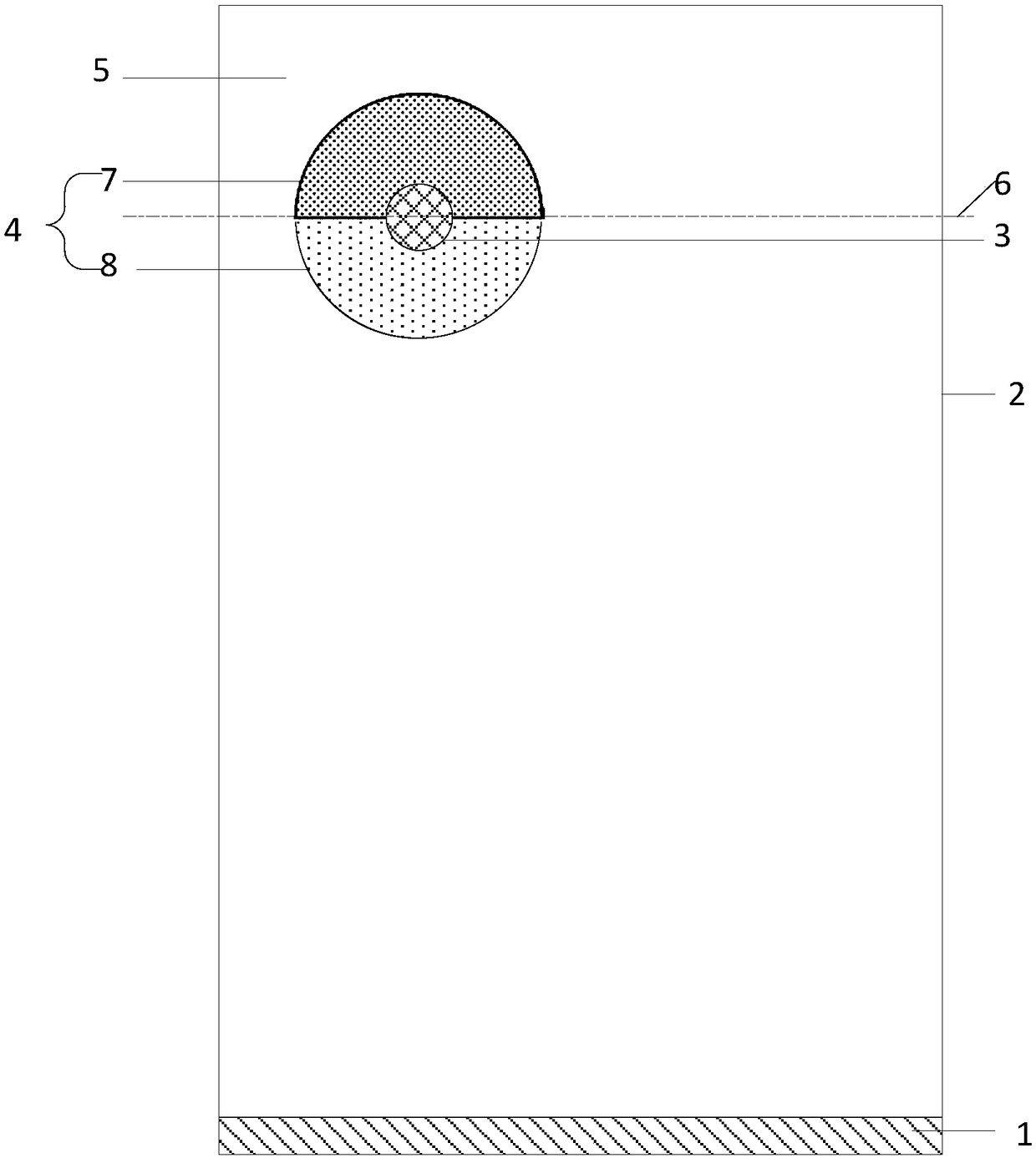
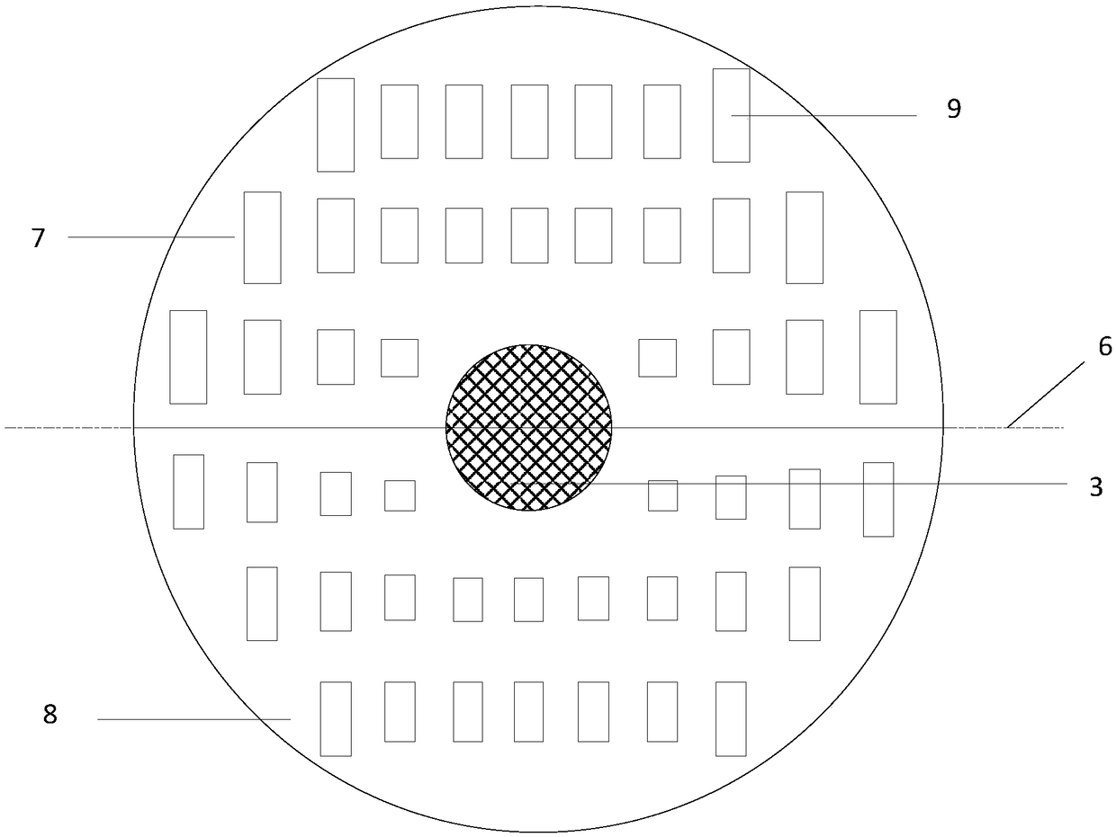
[0019] The embodiment of the application provides a display device, such as figure 1 As shown, the display panel includes a display panel and a backlight source 1 arranged on either side of the display panel; the display panel includes an array substrate 2, the array substrate 2 includes at least one hollow portion 3; the array substrate 2 has a first The display area 4 and the second display area 5, the first display area 4 surrounds the hollow portion 3, the boundary line of the first display area 4 and the second display area 5 and the edge of the hollow portion 3 The distance between is less than the preset value;

[0020] Along the axis line 6 of the hollow part, the first display area 4 is divided into a first sub-area 7 and a second sub-area 8. The first sub-area 7 is located at the far end of the backlight source 1, and The second sub-region 8 is located at the proximal end of the backlight source 1; that is, the first sub-region 7 is far away from the backlight source 1 ...


PUM


Abstract

The invention discloses a display device used to improve brightness uniformity of a display product. An embodiment of the invention provides a display device, including a display panel and a backlightarranged on any side of the display panel. The display panel comprises an array substrate, and the array substrate comprises at least a hollow-out portion. The array substrate has a first display region and a second display region. The first display region surrounds the hollow-out portion. Distances between boundary lines of the first display region and the second display region and the edge of the hollow-out portion are smaller than a preset value. An axial lead along the hollow-out portion divides the first display region into a first sub-region and a second sub-region. The first sub-regionis on a far end of the backlight. The second sub-region is on a near end of the backlight. Pixel aperture ratio of the first sub-region is larger than pixel aperture ratio of the second sub-region, and / or, penetration rate of pixels in the first sub-region is larger than penetration rate of pixels in the second sub-region.

Description

Technical field [0001] This application relates to the field of display technology, and in particular to a display device. Background technique [0002] With the development of the market, consumers have become more and more demanding on the display effect of the display. Not only the appearance design requirements are diversified, but also the requirements for the screen-to-body ratio are getting higher and higher. The full-screen technology is even without the ultra-narrow bezel. The frame design can achieve a screen-to-body ratio of ≥90%. With the body unchanged, the display area is maximized and the display effect is more stunning, which meets the needs of users. In the prior art, based on the structural design of the full screen, it is necessary to punch holes in the display area of ​​the panel to install the camera, earpiece, sensor, etc. However, when the full screen display product adopts a side backlight, the Hole, the light can not go directly to the back of the hole (...

Claims


Application Information

Patent Timeline
Patent Type & Authority Applications(China)
IPC IPC(8): G02F1/1362G02F1/1333G02F1/1335G02F1/1343G09F9/00
CPCG02F1/1333G02F1/133512G02F1/134309G02F1/136209G09F9/00
Inventor 卢丽君林丽敏李静邱英彰蔡寿金朱绎桦陈国照
Owner XIAMEN TIANMA MICRO ELECTRONICS
Why Eureka
Try Eureka