

Manufacturing method of a panel for liquid crystal
a liquid crystal display and manufacturing method technology, applied in the field of liquid crystal display manufacturing, can solve the problems of difference in electric characteristics, difference in the brightness between shots, and the appearance of shots at the boundary between shots
- Summary
- Abstract
- Description
- Claims
- Application Information
AI Technical Summary
Benefits of technology
Problems solved by technology
Method used
Image

Examples
first embodiment
[0028] FIG. 4 is a plan view showing a boundary area between shots of an LCD according to the present invention.
[0029] FIG. 5 is a plan view showing a unit stitch area of an LCD according to the first embodiment of the present invention.
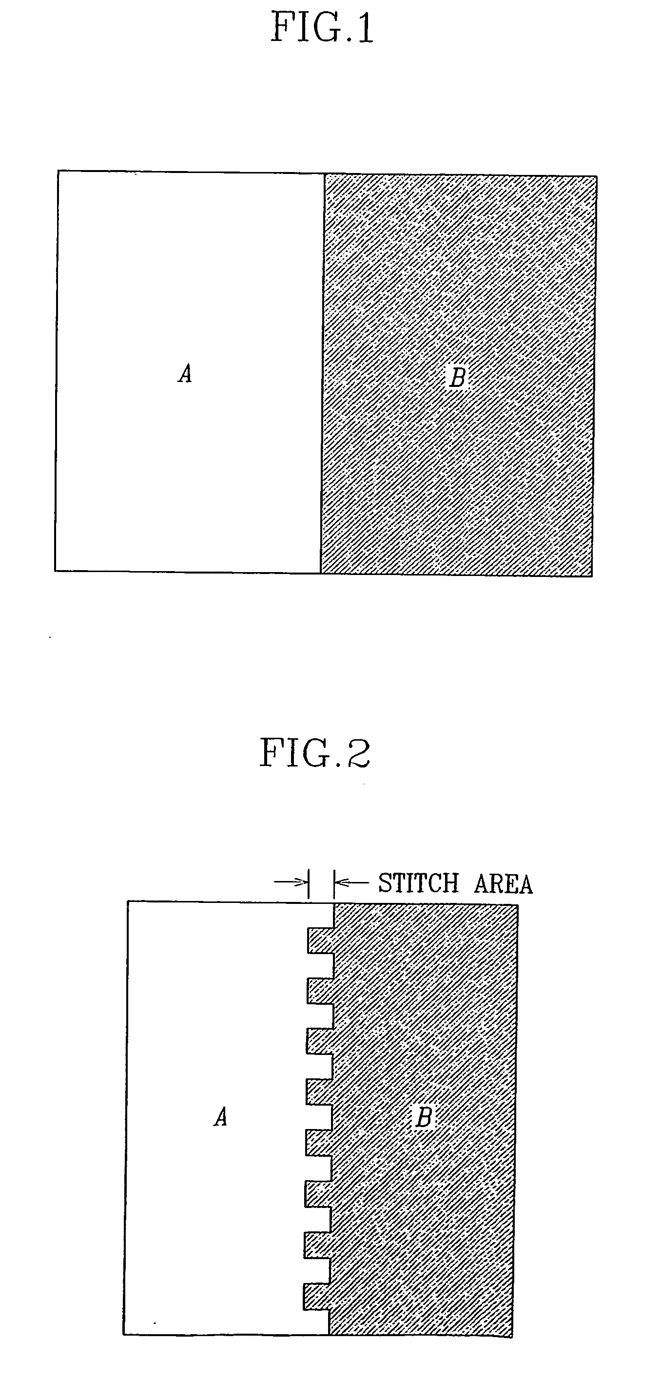
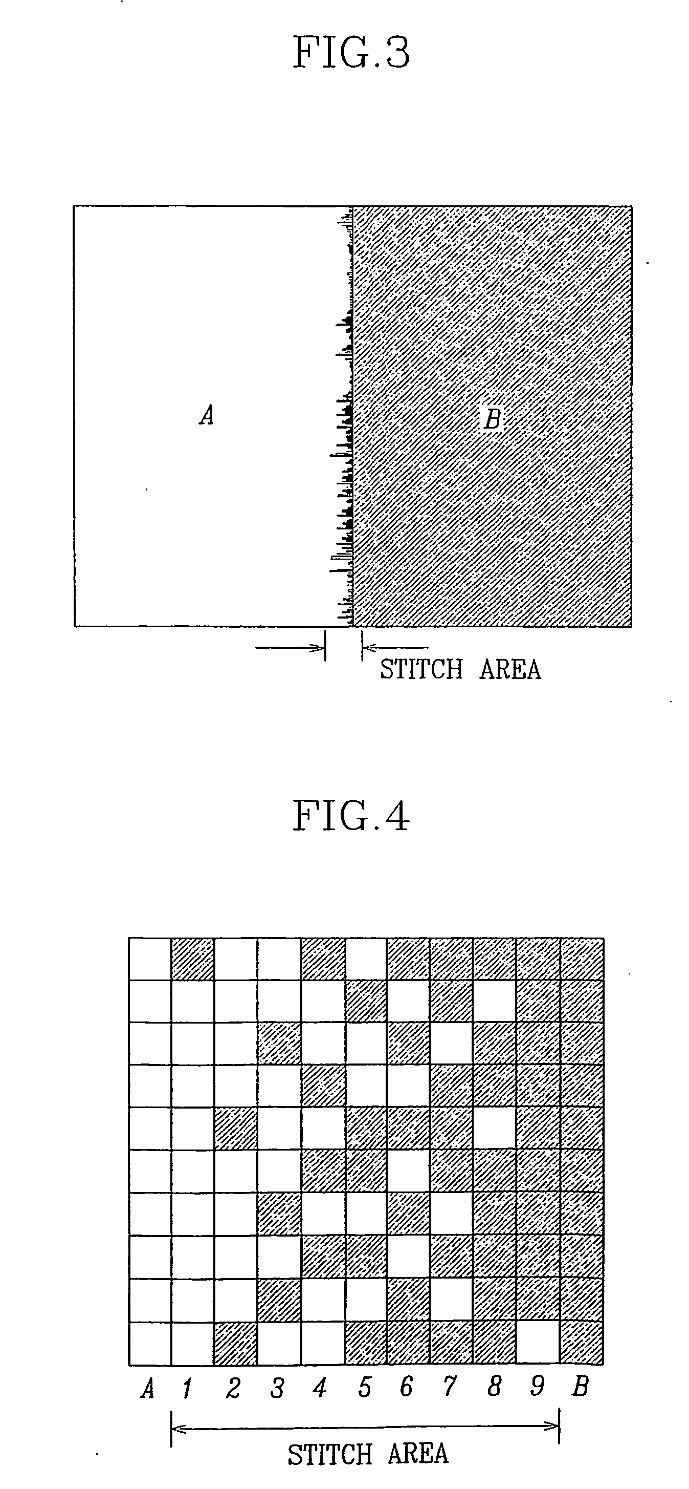
[0030] A stitch area is an overlapping area between two adjacent shots such as a left shot A (represented as a white area) and a light shot B (represented as a black area) as shown in FIG. 4. The stitch area is divided into a plurality of unit stitch areas, for example, 10.times.9 unit stitch areas as shown in FIG. 4. The unit stitch area refers to one basic area of the stitch area divided by n.times.m blocks (where n and m are natural numbers).
[0031] In this embodiment, a pixel includes two or more unit stitch areas. The reduced size of the unit stitch area prevents a mosaic pattern. As shown in FIG. 5, a pixel is divided into two areas a and b used as unit stitch areas according to the first embodiment of the present invention.
[0032] The unit stitc...
second embodiment
[0047] In this embodiment, a pixel includes two or more unit stitch areas. The reduced size of the unit stitch area prevents a mosaic pattern. As shown in FIG. 7, a pixel is divided into four areas a, b, c and d used as unit stitch areas according to the present invention.
[0048] Now, the unit stitch areas according to the second embodiment of the present invention will be described more in detail with reference to FIG. 7.
[0049] As shown in FIG. 7, a pixel area on a TFT array panel is defined by intersections of a plurality of gate lines 20 extending in a transverse direction and a plurality of data lines 70 extending in a longitudinal direction. A TFT and a pixel electrode 90 having a plurality of apertures 901, 903, 905, 907, 909, 911, and 913 are provided in each pixel area. A common electrode (not shown) having a plurality of apertures 401, 403, 405, 407, 409, 411 and 413 is formed on a color filter panel (not shown) opposite the TFT array panel. The apertures 401, 403, 405, 407,...
third embodiment
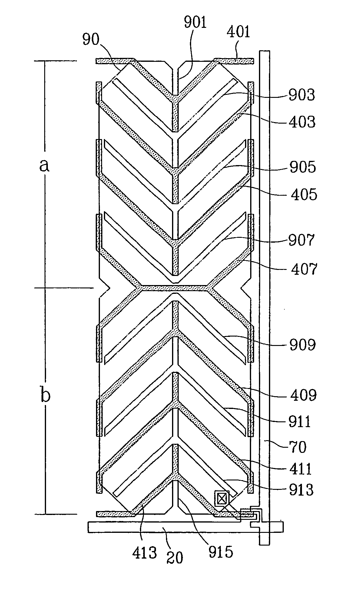
[0052] FIG. 10 is a plan view showing a unit stitch area of an LCD according to the present invention.
[0053] As shown in FIG. 10, a pixel area on a tin film transistor array panel is defined by intersections of a plurality of gate lines 20 extending in a transverse direction and a plurality of data lines 70 extending in a longitudinal direction. A TFT and a pixel electrode 90 having a plurality of apertures 901, 903, 905, 907, 909, 911, 913 and 915 are provided in each pixel area. A common electrode (not shown) having a plurality of apertures 401, 403, 405, 407, 409, 411, 413 and 415 is formed on a color filter panel (not shown) opposite the TFT array panel. The apertures 401, 403, 405, 407, 411, 413 and 415 on the common electrode are hatched. The apertures 901, 903, 905, 907, 909, 911, 913 and 915 of the pixel electrode 90 and the apertures 401, 403, 405, 407, 411, 413 and 415 of the common electrode are arranged in turns and partition the pixel area into a plurality of subareas. ...
PUM
 Abstract
Description
Claims
Application Information