Electro-optical device, and electronic apparatus and display driver IC using the same

a technology of electronic equipment and display devices, applied in the direction of identification means, instruments, computing, etc., can solve the problems of large differences in the delay of display control signals and luminance differences in the conventional art, and achieve the effect of decreasing the luminance difference in the screen

Inactive Publication Date: 2005-08-30
138 EAST LCD ADVANCEMENTS LTD
View PDF11 Cites 18 Cited by
  • Summary
  • Abstract
  • Description
  • Claims
  • Application Information

AI Technical Summary

Benefits of technology

[0012]Accordingly, an objective of the present invention is to provide an electro-optical device capable of decreasing the luminance difference in a screen even if a plurality of driver ICs are used to supply data signals electrodes, and an electronic apparatus and display driver IC using the electro-optical device.
[0020]The luminance difference in the conventional art is caused by a large difference in the delay of the display control signals between the master IC and the slave IC. This is because the master IC uses the display control signal generated therein, whereas the slave IC uses the display control signal input through an external wiring. The difference in the delay of the display control signals causes a difference between the voltages applied to the electrodes of the, display sections of the left screen 600A and the right screen 600B in FIG. 10, thereby causing the luminance difference.
[0021]According to the present invention, the display control signal supplied from the master IC is input to the master IC and at least one slave IC through an external wiring. Therefore, the luminance difference in a screen can be decreased by reducing the difference in the signal delay in the external wiring.
[0027]The timing of reading out the display data from the display memory and the timing of the data signal generated by the driver are both dependent upon the timing of the display control signal. The present invention can reduce the difference in these timings between the master IC and the slave IC can be reduced.
[0028]The present invention is particularly effective in the case of a gray scale display in the display section based on a pulse width modulation signal from the master IC and at least one slave IC. In this case, the display control signal generated in the display control signal generation section includes a gray scale control pulse for producing the pulse width modulation signal. The luminance difference in a screen can be reduced by decreasing the timing difference of the gray scale control pulses between the master IC and the slave IC.
[0029]According to a second aspect of the present invention, the display control signal generated in the master IC is delayed in an internal delay circuit whereas the display control signals delayed in an external wiring is used in the slave IC, thereby decreasing the difference in the delay between the display control signals used in the master IC and that used in the slave IC. This reduces the luminance difference in a screen.

Problems solved by technology

The luminance difference in the conventional art is caused by a large difference in the delay of the display control signals between the master IC and the slave IC.

Method used


Image

  • Electro-optical device, and electronic apparatus and display driver IC using the same
  • Electro-optical device, and electronic apparatus and display driver IC using the same
  • Electro-optical device, and electronic apparatus and display driver IC using the same

Examples


first embodiment

(Reason Why First Embodiment Decreases Luminance Difference in Screen)

[0098]On the contrary, according to this embodiment, the luminance difference in the conventional art shown in FIG. 10 can be decreased to such an extent that the difference is not significant visually. The reason will be described below.

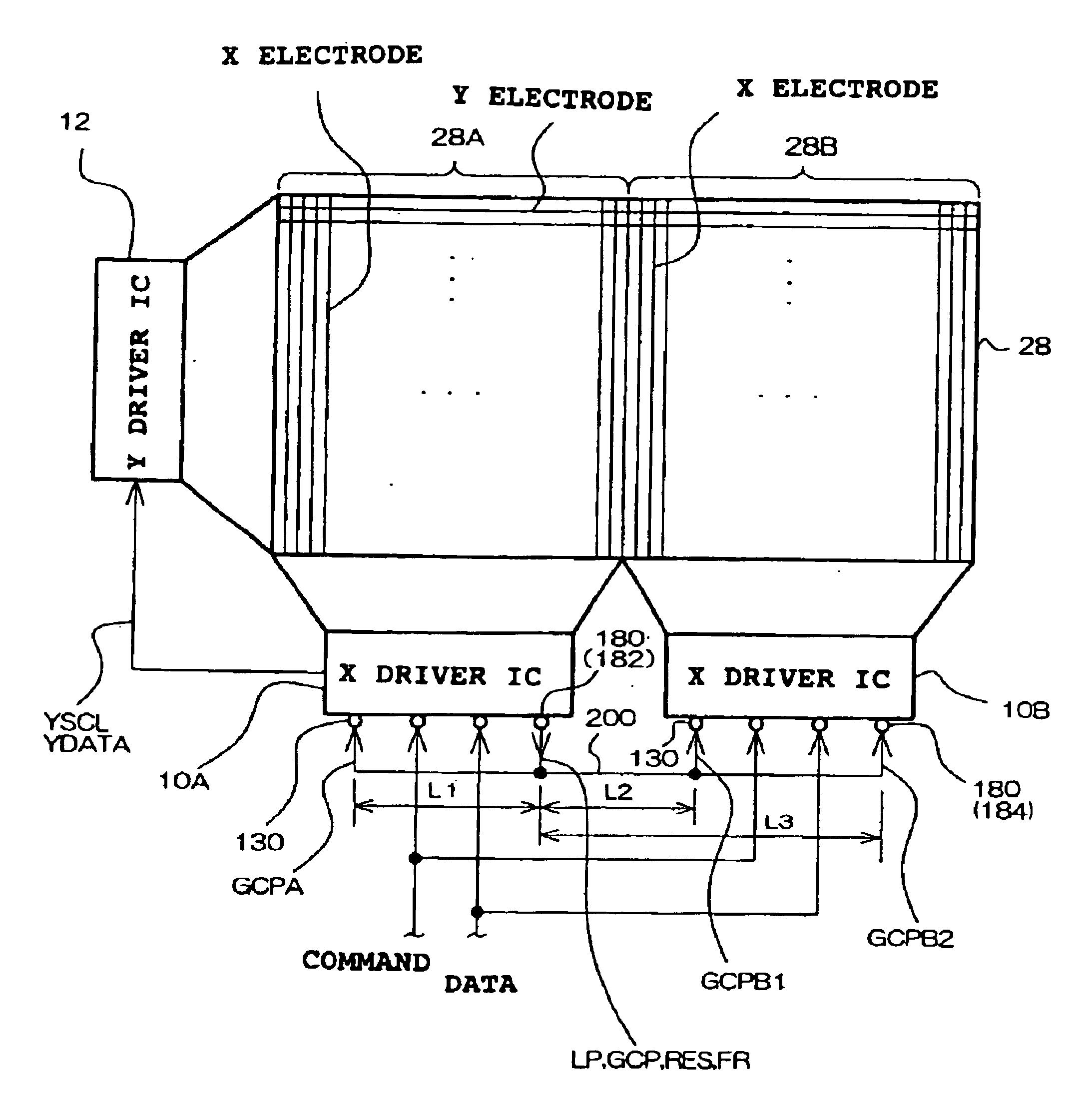
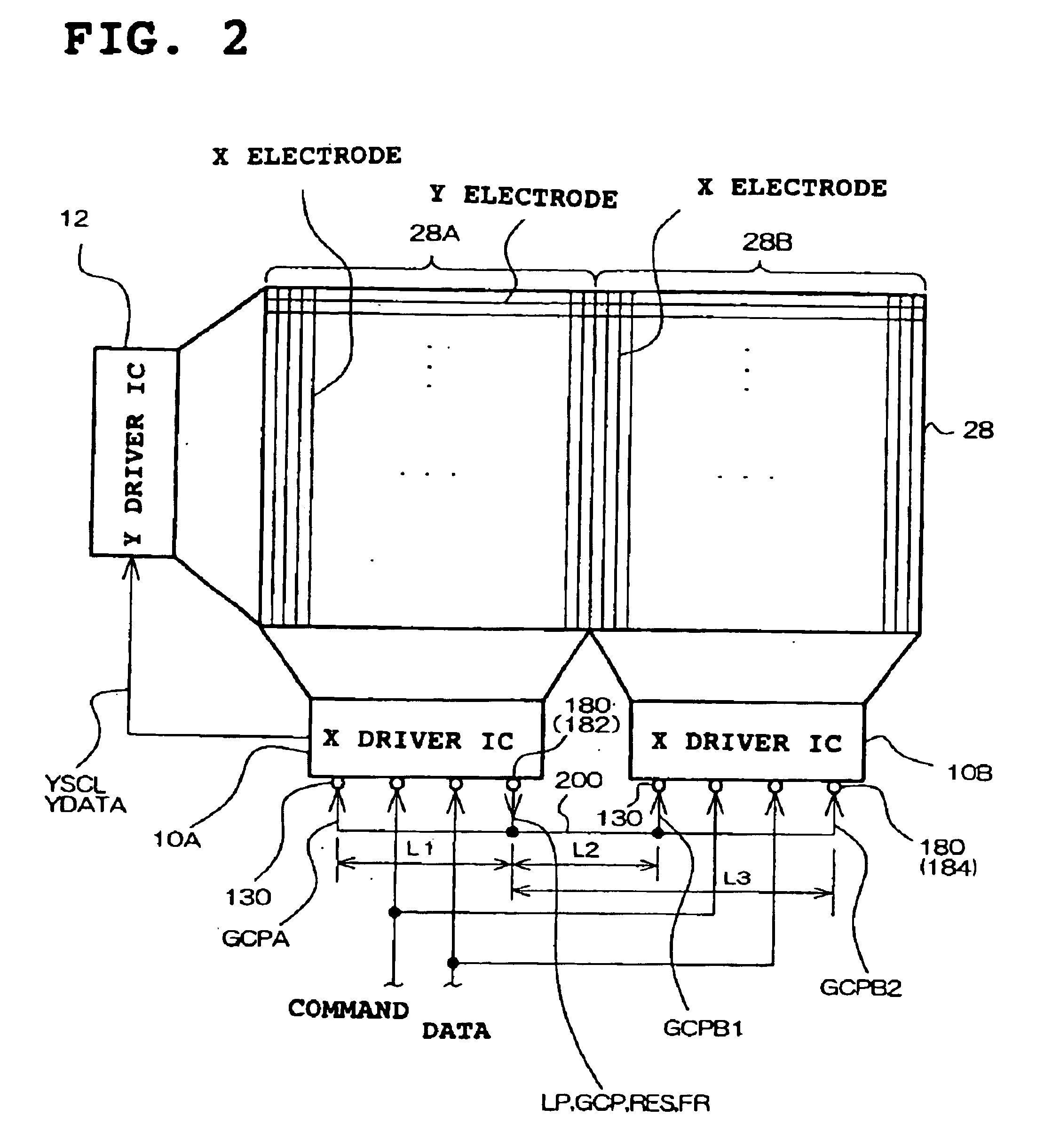
[0099]In FIG. 2, the length of the wiring between the output terminal 182 of the X driver IC 10A and the input terminal 130 of the X driver IC 10A is referred to as L1, and the lengths of the wiring between the output terminal 182 and the first and second input terminals 130 and 184 of the X driver IC 10B are referred to as L2 and L3. As is clear from FIG. 2, L1=L2

[0100]According to the above relation, the gray scale control pulses input to the first input terminal 130 of the X driver IC 10A and the first and second input terminals 130 and 184 of the X driver 10B are respectively referred to as GCPA, GCPB1, and GCPB2, as shown in FIG. 9.

[0101]As described above, the effective ...

second embodiment

[0106]FIG. 13 shows a second embodiment of the present invention in which the wiring 200 for the X driver ICs 10A and 10B differs from that in FIG. 2. In the second embodiment, the lengths of each region of the wiring 200 satisfy L21, and GCPB2 become as shown in FIG. 14.

[0107]Accordingly, it is understood that the gray scale control pulse GCPB2 having fall timing close to that of the gray scale control pulse GCPA used in the X driver 10A may be used.

[0108]In the case shown in FIGS. 13 and 14, an OR-gate may be used as the selection circuit 140 shown in FIG. 3, where the logical OR between the gray scale control pulses GCPB1 and GCPB2 is carried out, thereby selecting the falling edge of the gray scale control pulse GCPB2 as shown in FIG. 14.

[0109]FIG. 15 shows an example in which three X driver ICs 10A, 10B, and 10C are connected. The center X driver IC 10A may be the master and both the X driver ICs 10B and 10C adjacent to the X driver IC 10A may be the slaves. In this case, the d...

third embodiment

[0111]FIG. 17 shows a liquid crystal device according to a third embodiment of the present invention. As shown in FIG. 17, display control signals output from an input / output terminal 180 (output terminal 182) of an X driver IC 400A as a master are input to an X driver IC 400B as a slave through a first input terminal 130 and a second input terminal 184 (input / output terminal 180) of the X driver 400B.

[0112]FIGS. 18 and 19 show block diagrams of part of the X driver ICs 400A and 400B shown in FIG. 17. Parts having the same function as those in the block diagrams shown in FIGS. 6 and 7 are represented by the same symbols, and description thereof will be omitted.

[0113]The X driver IC 400A shown in FIG. 18 and the X driver IC 400B shown in FIG. 19 have the same structure, and differ in their function by the logic input to an M / S selection terminal 162.

[0114]These driver ICs 400A and 400B differ from those shown in FIGS. 6 and 7 in that the internal structure of an input / output-switchin...


PUM

PropertyMeasurementUnit
sizeaaaaaaaaaa
sizeaaaaaaaaaa
voltageaaaaaaaaaa

Abstract

A liquid crystal device having a display section provided with a plurality of X electrodes and a plurality of Y electrodes, a master X driver IC and a slave X driver IC for driving the X electrodes, and a Y driver for driving the Y electrodes. The master IC has a display control signal generation section which generates a display control signal based on a signal from an external MPU and an output terminal (or input / output terminal) which outputs the display control signal. Each of the master IC and slave IC has an input terminal for receiving the display control signal from the master IC through an external wiring. This liquid crystal device can eliminate a luminance difference within the display screen driven by the master IC and the slave IC.

Description

BACKGROUND OF THE INVENTION[0001]1. Field of the Invention[0002]The present invention relates to an electro-optical device using an electro-optical element such as a liquid crystal, and to an electronic apparatus and a display driver IC using the electro-optical device.[0003]2. Description of Related Art[0004]A liquid crystal display displays a monochrome display or a gray scale display including halftone, for example.[0005]When a liquid crystal element is used as an electro-optical element and driven passively or actively, one of a plurality of row electrodes (Y electrodes) extending in a lateral direction is selected and data signals are supplied to a plurality of column electrodes (X electrodes) extending in a longitudinal direction simultaneously, thereby driving the liquid crystal for a line at a time.[0006]In recent years, there has been a tendency to increase the number of X electrodes to provide an extremely fine display.[0007]In this case, it is difficult to drive all X ele...

Claims


Application Information

Patent Timeline
Patent Type & Authority Patents(United States)
IPC IPC(8): G09G3/36G02F1/133G09F9/00G09G3/20
CPCG09G3/3666G09G3/3685G09G3/2014G09G3/3614G09G3/3692G09G2310/0221G09G2320/0233G09G3/36
Inventor ISHIYAMA, HISANOBU
Owner 138 EAST LCD ADVANCEMENTS LTD
Why Eureka
Try Eureka