Supercharge Your Innovation With Domain-Expert AI Agents!

Lower electrode device and reaction chamber

A technology of electrode device and electrode plate, which is applied in the direction of circuits, discharge tubes, electrical components, etc., can solve the problems of exceeding the power ratio range, unable to meet the uniformity of etching, etc., and achieve the effect of meeting the requirements of uniformity of etching

Active Publication Date: 2020-02-21
BEIJING NAURA MICROELECTRONICS EQUIP CO LTD
View PDF7 Cites 0 Cited by
  • Summary
  • Abstract
  • Description
  • Claims
  • Application Information

AI Technical Summary

Problems solved by technology

[0004] However, in order to meet the requirements of etching uniformity, the power ratio of the RF power loaded on the coil 12 and the lower electrode 14 can only be kept within a specific range, which brings great challenges to the application of the etching process. Limitations. In practical applications, in order to meet different process requirements, the RF power supplies on the coil 12 and the lower electrode 14 need to be loaded with different powers, which will cause the specific power ratio range to be exceeded, and the etching uniformity requirements cannot be met.

Method used


Image

  • Lower electrode device and reaction chamber
  • Lower electrode device and reaction chamber
  • Lower electrode device and reaction chamber

Examples


Embodiment Construction

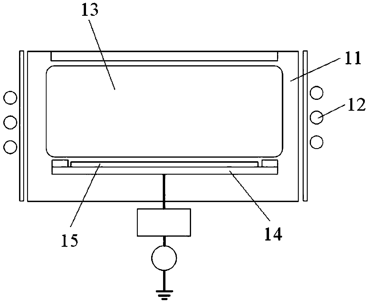
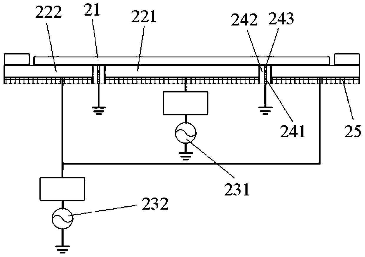
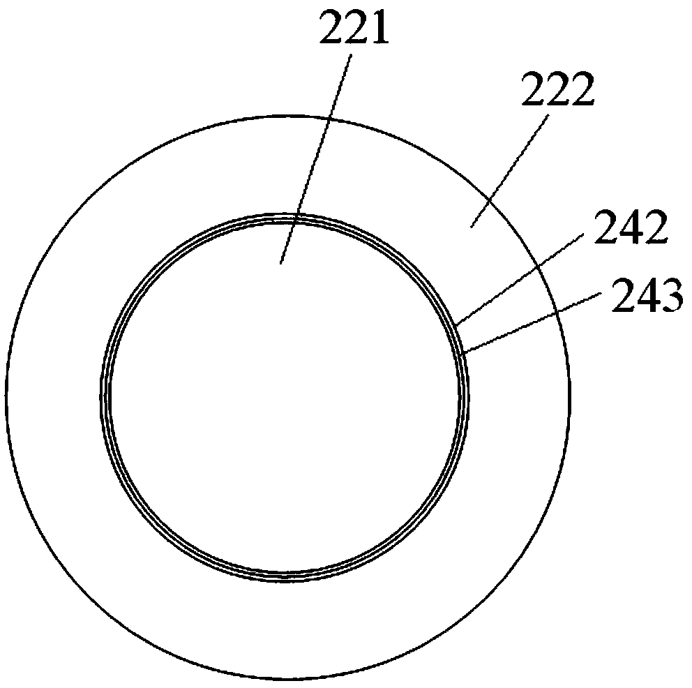
[0033] In order for those skilled in the art to better understand the technical solution of the present invention, the lower electrode device and the reaction chamber provided by the present invention will be described in detail below in conjunction with the accompanying drawings.

[0034] like Figure 2-Figure 5 As shown, this embodiment provides a lower electrode device, including an electrode plate, the electrode plate includes a plurality of sub-plates, and by applying different bias powers to the multiple sub-plates, the substrate corresponding to the multiple sub-plates can be adjusted. 21 etch uniformity across multiple regions. Furthermore, by dividing the electrode plate into a plurality of sub-plates, the bias power loaded on the electrode plate can be controlled in partitions, so that at least two sub-plates can be divided according to the actual distribution of the etching rate on the surface of the substrate 21. The plates are loaded with different bias powers to...


PUM


Abstract

The invention provides a lower electrode device and a reaction chamber. The lower electrode device comprises an electrode plate, the electrode plate comprises a plurality of sub-electrode plates, andetching uniformity of a plurality of areas of a substrate corresponding to the plurality of sub-electrode plates is adjusted by loading different bias power to the plurality of sub-electrode plates. According to the invention, when the etching uniformity requirement is satisfied, different process requirements are met.

Description

technical field [0001] The invention relates to the field of microelectronics manufacturing, in particular to a lower electrode device and a reaction chamber. Background technique [0002] At present, in the field of microelectronics manufacturing, due to the excellent directionality and selectivity of the plasma process, it has become the best choice for the manufacture of microelectronic devices and has been widely used. It bombards the surface of the substrate with plasma, thereby The surface of the substrate is etched, and after the plasma etching process, the uniformity of the etching amount on the substrate surface is a key indicator for testing the quality of the plasma etching process. [0003] like figure 1 As shown, an existing plasma chamber includes a reaction chamber 11, a coil 12, a plasma 13 and a lower electrode plate 14. When performing an etching process, the process gas is passed into the reaction chamber 11, and the coil 12 Load a radio frequency power ...

Claims


Application Information

Patent Timeline
IPC IPC(8): H01J37/32H01L21/3065
CPCH01J37/32532H01J37/32458H01L21/3065H01J2237/04H01J2237/334
Inventor 苏振宁
Owner BEIJING NAURA MICROELECTRONICS EQUIP CO LTD
Features
  • R&D
  • Intellectual Property
  • Life Sciences
  • Materials
  • Tech Scout
  • Unparalleled Data Quality
  • Higher Quality Content
  • 60% Fewer Hallucinations
Learn More