
Ceramic photoelectric coupler and manufacturing method thereof

A technology of optocoupler and manufacturing method, applied in the direction of final product manufacturing, sustainable manufacturing/processing, circuits, etc., can solve the problems of complex production process, cumbersome packaging process, complex structure, etc., achieve mechanical shock resistance and reduce process assembly Difficulty, size reduction effect

Pending Publication Date: 2020-02-21
NO 43 INST OF CHINA ELECTRONICS TECH GRP CETC
View PDF0 Cites 2 Cited by
  • Summary
  • Abstract
  • Description
  • Claims
  • Application Information

AI Technical Summary

Problems solved by technology

The structure of the optocoupler device in the prior art is complex, the production process is complex, and the packaging process is relatively cumbersome

Method used


Image

  • Ceramic photoelectric coupler and manufacturing method thereof
  • Ceramic photoelectric coupler and manufacturing method thereof
  • Ceramic photoelectric coupler and manufacturing method thereof

Examples


Embodiment Construction

[0024] The present invention will be further described below in conjunction with accompanying drawing:

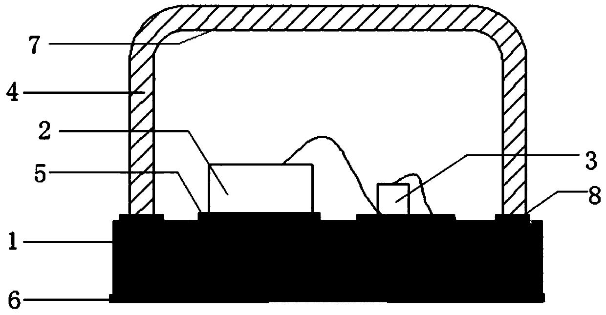
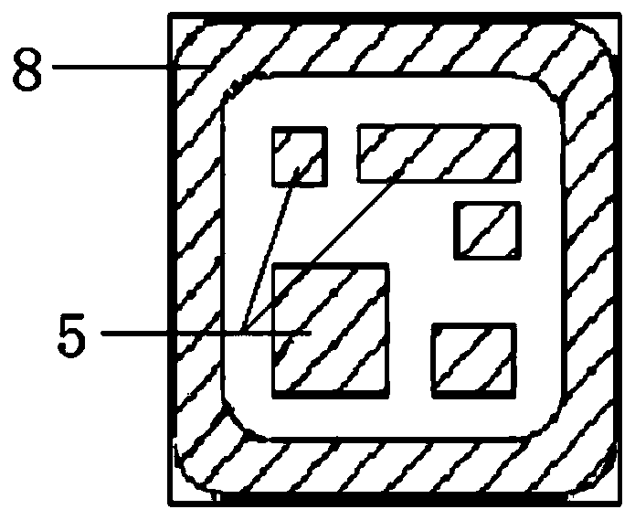
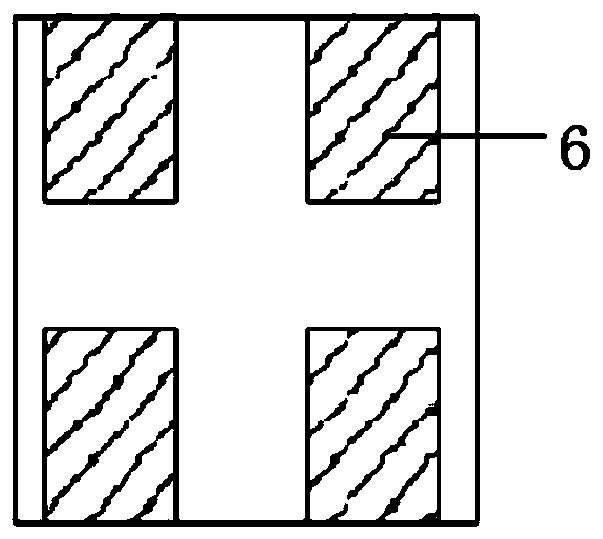
[0025] like Figure 1-3 As shown, the ceramic optocoupler of the present embodiment includes a multilayer ceramic substrate 1 and a metal cap 4 which is arranged on the ceramic substrate 1 and forms a sealed cavity with the upper surface of the ceramic substrate 1. There is a metallization area 8 for welding the metal cap 4 and a metallization area 5 for connecting components. The metallization area 8 and the metal cap 4 are connected by gold-tin welding to realize integrated sealing. A light-emitting diode 3 and a phototransistor 2 are installed on the multilayer ceramic substrate 1, and different electrodes of the light-emitting diode 3 and the phototransistor 2 are respectively electrically connected to the specific metallization area 5 on the upper surface of the multilayer ceramic substrate 1; the multilayer ceramic substrate The metallization 5 on the upper surface i...


PUM

PropertyMeasurementUnit
thicknessaaaaaaaaaa
electrical resistanceaaaaaaaaaa

Abstract

The invention relates to a ceramic photoelectric coupler and a manufacturing method thereof. The coupler comprises a multilayer ceramic substrate and a metal cover cap which is arranged on the ceramicsubstrate, wherein a sealed cavity is formed by the metal cover cap and the upper surface of the ceramic substrate. The upper surface and the lower surface of the ceramic substrate are provided witha number of metallized regions respectively. Different metallized regions on the upper surface of the multilayer ceramic substrate are electrically communicated with corresponding different metallizedregions on the lower surface of the multilayer ceramic substrate. Light emitting diodes and phototriodes, electrically communicated with the metallized regions, are arranged in the metallized regionson the upper surface of the multilayer ceramic substrate. According to the invention, internal wiring and precise circuit layout of the multilayer ceramic substrate are adopted; the multilayer ceramic substrate is directly used as a packaging base; internal optical path transmission is achieved through the structural design of a packaging cavity and a reflective coating arranged in the cover cap;the phenomenon that optical path transmission is affected by cracking and layering of light guide glue is avoided; the transmission efficiency and stability of the reflective photoelectric coupler are improved; and the process assembly difficulty is reduced.

Description

technical field [0001] The invention relates to the field of photoelectric technology, in particular to a ceramic photocoupler and a manufacturing method thereof. Background technique [0002] The photocoupler is generally composed of three parts: light emission, light reception and signal amplification. The photocurrent is further amplified and then output, thereby completing the conversion of electricity-light-electricity, and playing the role of input, output, and isolation. Since the input and output of the optocoupler are isolated from each other, and the electrical signal transmission has the characteristics of unidirectionality, it has good electrical insulation ability and anti-interference ability. [0003] Most of the existing optocouplers are plastic-encapsulated devices, but for high-quality military-grade optocouplers, they need to work in the full military-standard temperature range of -55°C to 125°C, and the epoxy plastic encapsulation material cannot effecti...

Claims


Application Information

Patent Timeline
Patent Type & Authority Applications(China)
IPC IPC(8): H01L31/12H01L31/02H01L31/0203H01L31/18
CPCH01L31/125H01L31/02005H01L31/0203H01L31/18Y02P70/50
Inventor 朱雨生雷子薇李林森王斌
Owner NO 43 INST OF CHINA ELECTRONICS TECH GRP CETC
Learn More