Method for reducing heterogeneous three-dimensional network-on-chip layout power consumption
An on-chip network and power consumption technology, applied in the field of integrated circuits, can solve problems such as difficulty in selecting a better solution, interference from human factors, and few layout solutions
- Summary
- Abstract
- Description
- Claims
- Application Information
AI Technical Summary
Problems solved by technology
Method used
Image

Examples
Embodiment Construction
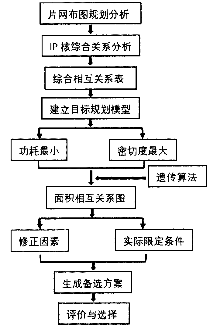
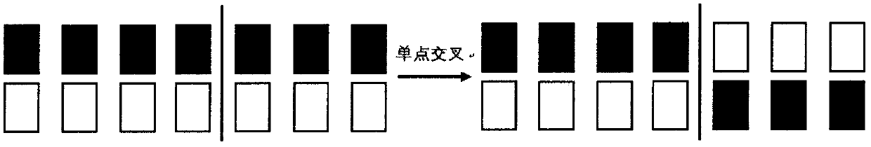
[0018] stepl SLP combined with genetic algorithm
[0019] The SLP method has the characteristics of strong logic and clear organization. In order to solve the above-mentioned deficiencies of the traditional SLP, after obtaining the objective function, we use the genetic algorithm to solve it, avoiding the interference of human factors. The specific steps of the method for improving SLP in this paper are as follows: figure 1 Shown:
[0020] Model establishment of step2 layout planning
[0021] A. Model assumptions
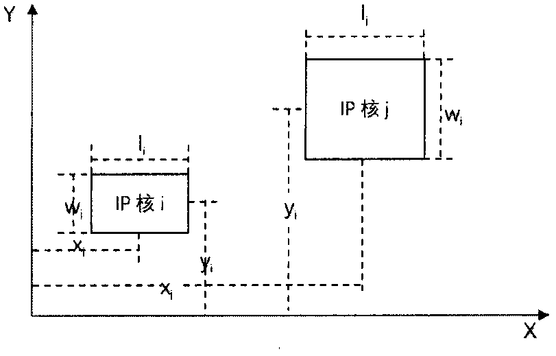
[0022] The main goal of the on-chip network layout design in this paper is to achieve the minimum communication power consumption between IP cores and the maximum comprehensive relationship. The research object of the paper is to establish a layout optimization model of a three-dimensional network-on-chip. The assumptions required for the model are listed here.
[0023] (1) The scope of the general layout planning area of the three-dimensional sheet network ...
PUM
 Abstract
Description
Claims
Application Information
 - R&D Engineer
- R&D Manager
- IP Professional
- Industry Leading Data Capabilities
- Powerful AI technology
- Patent DNA Extraction
Browse by: Latest US Patents, China's latest patents, Technical Efficacy Thesaurus, Application Domain, Technology Topic.
© 2024 PatSnap. All rights reserved.Legal|Privacy policy|Modern Slavery Act Transparency Statement|Sitemap