Memory chip reset method and imaging device

A reset method and memory chip technology, applied in printing and other directions, can solve the problems of low reset success rate, waste, chip waste, etc., and achieve the effect of high reset success rate, reducing waste and alleviating economic pressure.

Active Publication Date: 2021-09-07
GUANGZHOU ZHONO ELECTRONICS TECH CO LTD
View PDF12 Cites 0 Cited by
  • Summary
  • Abstract
  • Description
  • Claims
  • Application Information

AI Technical Summary

Problems solved by technology

[0003] With the popularization of imaging equipment, the consumption of imaging equipment consumables is also increasing, but after the toner cartridge or the toner in the ink cartridge is consumed, the remaining amount of consumables recorded in the consumable chip will become zero, resulting in The chips on the toner cartridge or ink cartridge are discarded together with the waste toner box and cannot be reused, resulting in waste
[0004] Although the chip recycler will reset the discarded old chips to realize the reuse of discarded chips, the existing reset method, for the old chips with a high degree of encryption, has a low reset success rate, which will still cause chip damage. waste

Method used


Image

  • Memory chip reset method and imaging device
  • Memory chip reset method and imaging device
  • Memory chip reset method and imaging device

Examples


Embodiment Construction

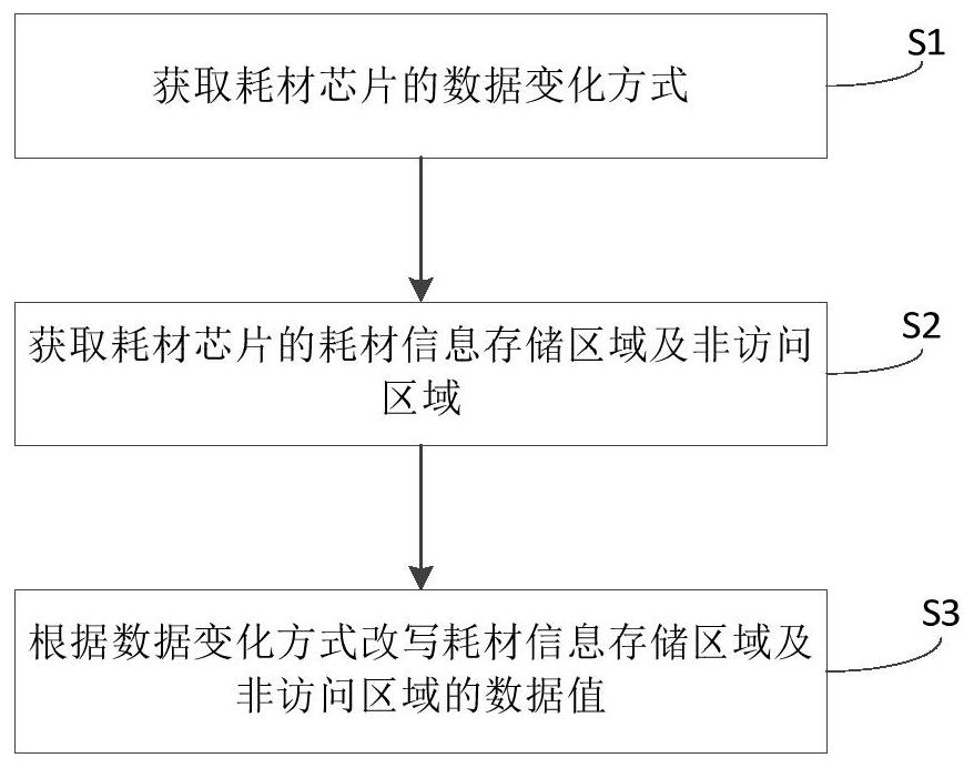
[0023] Embodiments of the present invention are described in detail below, and the embodiments described with reference to the drawings are exemplary, and embodiments of the present invention are described in detail below.

[0024] The communication rules between imaging devices such as printers and consumable chips are as follows: when the printer is turned on, the printer and consumable chips pass a certain communication protocol, such as IIC (Inter-Integrated Circuit, integrated circuit bus), UART (Universal Asynchronous Receiver / Transmitter, universal Asynchronous transceiver transmitter) communicates with the consumable chip to verify the legitimacy of the consumable box and the information about the consumable box stored in the consumable chip. The legitimacy of the consumables box is mainly reflected by some encryption algorithms. That is to say, the data values ​​of the printer and the consumable chip are encrypted, and the data value can be decrypted only by knowing t...


PUM


Abstract

The present invention proposes a method for resetting a memory chip and an imaging device. The method for resetting a memory chip includes: acquiring the data change mode of the consumable chip; acquiring the consumable information storage area and non-access area of ​​the consumable chip; according to the data change mode Rewriting the data values ​​stored in the consumables information storage area and the non-access area, wherein, rewriting the stored data values ​​in the consumables information storage area is the initial data value, and changing the data values ​​stored in the non-access area according to the data change mode; wherein , the address of the non-access area is adjacent to the address of the consumables information storage area. The storage chip resetting method of the present invention, by acquiring the data change mode of the consumable chip and the consumable information storage area and non-access area of ​​the consumable chip, rewrites the data values ​​of the consumable chip access area and non-access area according to the rewriting rules to realize the storage chip reset.

Description

technical field [0001] The invention relates to the field of chip technology, in particular to a method for resetting a memory chip and an imaging device. Background technique [0002] Imaging equipment, such as printers, photocopiers, fax machines, word processors or multi-functional all-in-one machines, etc., are equipped with detachable consumable boxes that are convenient for users to replace. Usually, consumable chips need to be installed on the consumable boxes. Through the consumable chips and The imaging device communication of the imaging device enables the imaging device to ideally use the consumable box and its consumables such as toner and ink. The consumables chip stores the program and consumables box data, and the consumables box data can include version number, model, remaining consumables, etc. [0003] With the popularization of imaging equipment, the consumption of imaging equipment consumables is also increasing, but after the toner cartridge or the tone...

Claims


Application Information

Patent Timeline
Patent Type & Authority Patents(China)
IPC IPC(8): B41J2/175
CPCB41J2/175
Inventor 刘杏肖其他发明人请求不公开姓名
Owner GUANGZHOU ZHONO ELECTRONICS TECH CO LTD
Why Eureka
Try Eureka