Read-only memory and its manufacture

A technology of read-only memory and control gate, which is applied in semiconductor/solid-state device manufacturing, electrical solid-state devices, semiconductor devices, etc., and can solve problems such as increasing the complexity of the manufacturing process, unstable manufacturing process, and easy excessive etching

Inactive Publication Date: 2003-12-31
TAIWAN SEMICON MFG CO LTD
View PDF0 Cites 0 Cited by
  • Summary
  • Abstract
  • Description
  • Claims
  • Application Information

AI Technical Summary

Problems solved by technology

[0008] In the existing flash memory, when defining the first polysilicon layer to form the floating gate and defining the second polysilicon layer to form the control gate, since there is no etch barrier layer on the source / drain region of the semiconductor substrate, Therefore, when removing the first polysilicon layer and the second polysilicon layer, it is easy to etch too much and form a trench in the source / drain region
People have used the existing technology to solve the above problems, using the manufacturing process to control the depth of the trench, but this kind of manufacturing process is relatively unstable, it is difficult to accurately control the depth of the trench, and it will limit the depth of the source / drain junction; Limiting and implanting arsenic ions at the position where the trench is formed, so that a sufficiently thick etching barrier layer grows, this method needs to increase the mask, which will increase the complexity of the manufacturing process; and use the floating gate as a mask layer to process the arsenic Ion implantation to grow a sufficiently thick etching barrier layer, because the thick oxide layer on the sidewall of the floating gate will make the floating gate and the control gate have a lower coupling rate (Coupling Rate)

Method used


Image

  • Read-only memory and its manufacture
  • Read-only memory and its manufacture
  • Read-only memory and its manufacture

Examples


Embodiment Construction

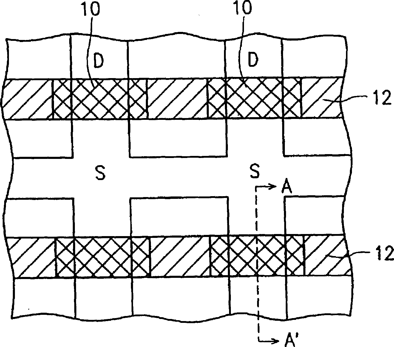
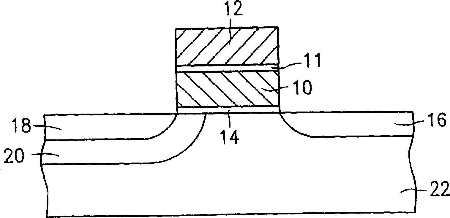
[0024] see image 3 , which is a top view of the structure of the flash memory in a preferred embodiment of the present invention, wherein the forward slashed floating gate and the backslashed control gate are perpendicular to each other, and the area where the floating gate and the control gate overlap represents a memory cell. and please refer to Figure 4a to Figure 4h ,in Figure 4f for along image 3 Schematic cross-sectional view of the structure of the AA' line of the flash memory, Figure 4g for along image 3 Schematic cross-sectional view of the structure of the BB' line of the medium flash memory, Figure 4h for along image 3 A schematic cross-sectional view of the structure of the CC' line of the flash memory, Figure 4a to Figure 4f A schematic diagram illustrating the manufacturing process of the flash memory in a preferred implementation of the present invention.

[0025] First, please refer to Figure 4a and cooperate image 3In order to manufacture t...


PUM


Abstract

The manufacture of read-only memory includes forming seccessively tunneling oxide layer, the first polycrystalline silicon layer, bottom oxide layer and the first silicon nitride layer on the semiconductor substrate; mask-delimiting the polycrystalline silicon layer as floating grid; forming doping area in the substrate, top oxide layer and the second silicon nitride layer on the first silicon nitride layer; etching back the second silicon nitride layer and forming barrier wall of silicon nitride on the side wall of the floating grid; forming etching barrier layer in oxidizing-doping area, forming silicon nitroxide layer in barrier wall, forming the second polycrystalline silicon layer and delimiting control grid; and doping to form the source area and drain area.

Description

technical field [0001] The invention relates to a manufacturing method of a semiconductor element, in particular to a read-only memory and its manufacturing method. Background technique [0002] Read-only memory (Read Only Memory-ROM) is a kind of permanent memory (Non-Volatile Memory), and the stored information or data will not disappear due to power supply interruption. Erasable Programmable ROM (Erasable Programmable ROM-ERPOM) is to extend the application of ROM to delete and rewrite data, but the action of deleting needs to use ultraviolet light, so the packaging cost of EPROM is relatively high. high. In addition, when EPROM deletes data, it will delete all the programs or data stored in ERPOM, which makes it necessary to start over every time the data is modified, which is quite time-consuming. [0003] Another kind of electrically erasable and programmable read-only memory (Electrically Erasable Programmable ROM-EEPROM) that allows partial modification of data doe...

Claims


Application Information

Patent Timeline
Patent Type & Authority Patents(China)
IPC IPC(8): H01L21/82H01L21/8246H01L27/112
Inventor 张格荥
Owner TAIWAN SEMICON MFG CO LTD
Why Eureka
Try Eureka