High-voltage LED chip and manufacturing method thereof

A technology of LED chip and manufacturing method, which is applied in the direction of electrical components, electric solid devices, circuits, etc., can solve problems such as current pulse surge and high-voltage LED chip burnout, achieve balance stress, improve the ability to resist pulse current impact, and reduce impact Effect

Pending Publication Date: 2020-04-03
FOSHAN NATIONSTAR SEMICON
View PDF0 Cites 2 Cited by
  • Summary
  • Abstract
  • Description
  • Claims
  • Application Information

AI Technical Summary

Problems solved by technology

Household circuits often have problems with current surges, which can easily cause high-voltage LED chips to burn out

Method used


Image

  • High-voltage LED chip and manufacturing method thereof
  • High-voltage LED chip and manufacturing method thereof
  • High-voltage LED chip and manufacturing method thereof

Examples


Embodiment Construction

[0031] In order to make the object, technical solution and advantages of the present invention clearer, the present invention will be further described in detail below in conjunction with the accompanying drawings.

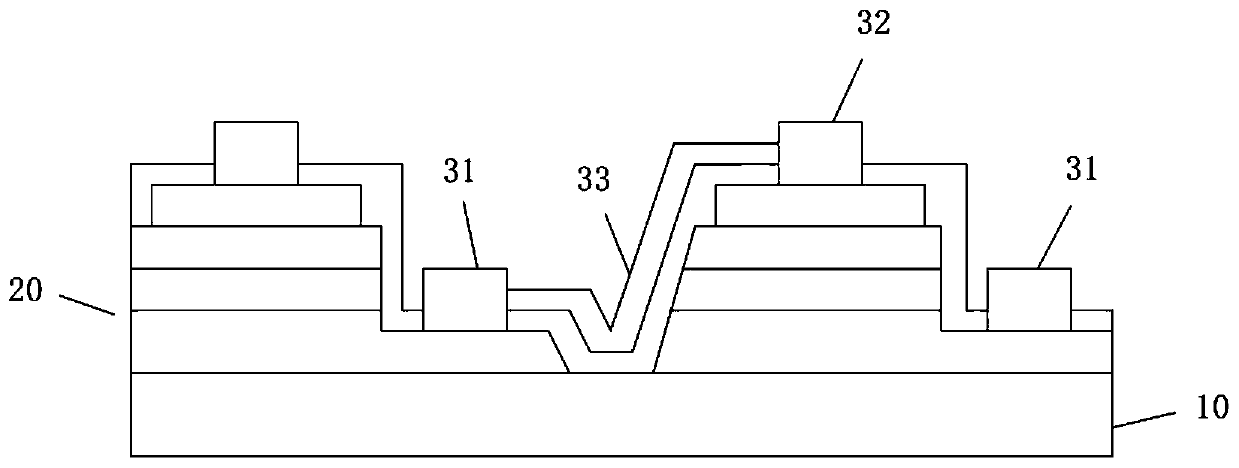
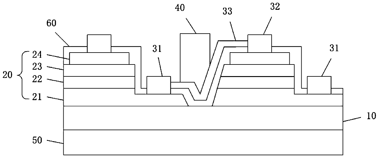
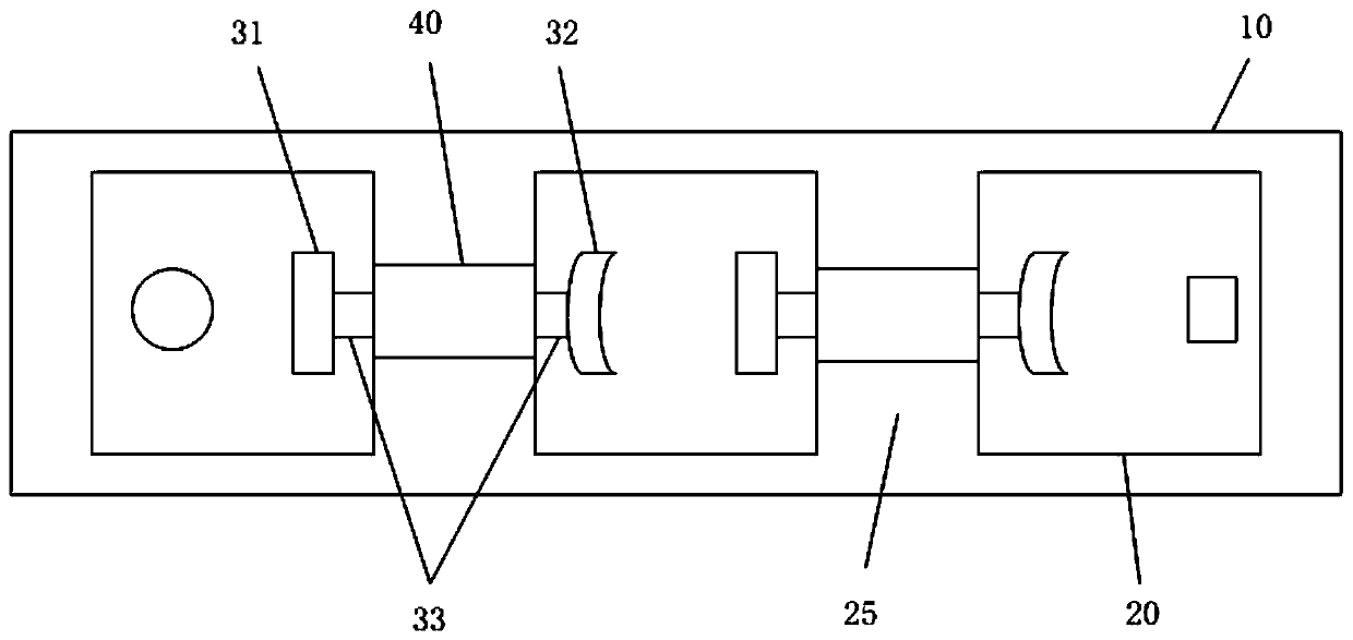
[0032] see figure 2 and image 3 A high-voltage LED chip provided by the present invention includes a substrate 10 , several light-emitting structures 20 disposed on the front surface of the substrate 10 , N electrodes 31 , P electrodes 32 , connection electrodes 33 , and a bridging strengthening layer 40 .

[0033] The substrate 10 of the present invention is preferably a sapphire substrate. The light-emitting structure 20 of the present invention includes an epitaxial layer and a transparent conductive layer 24, and the epitaxial layer includes a first semiconductor layer 21 and a second semiconductor layer sequentially arranged on the substrate 10. 22 and the second semiconductor layer 23. Preferably, the material of the epitaxial layer in the present invent...


PUM

PropertyMeasurementUnit
thicknessaaaaaaaaaa
thicknessaaaaaaaaaa
thicknessaaaaaaaaaa

Abstract

The invention discloses a high-voltage LED chip and a manufacturing method thereof. The chip comprises a substrate, a plurality of light-emitting structures arranged on the front surface of the substrate, N electrodes, P electrodes, a connecting electrode and a bridging reinforcing layer, wherein the N electrodes and the P electrodes are arranged on the light-emitting structures; the bridging strengthening layer comprises a Cr layer, a Ti layer, a Pt layer and an Au layer, the Cr layer is arranged between the connecting electrode and the Ti layer, and the Pt layer is arranged between the Ti layer and the Au layer; the N electrodes and the P electrodes of every two adjacent light-emitting structures are conductively connected through the connecting electrode, and the bridging strengtheninglayer is arranged on the connecting electrode so as to strengthen the connecting electrode and shunt a current passing through the connecting electrode. According to the invention, the bridging strengthening layer is arranged on the connecting electrode, so that only the current flowing through the connecting electrode can be shunted to the bridging strengthening layer, the impact of pulse currenton the bridging part of the connecting electrode is reduced, and the pulse current impact resistance of the chip is improved.

Description

technical field [0001] The invention relates to the technical field of light-emitting diodes, in particular to a high-voltage LED chip and a manufacturing method thereof. Background technique [0002] Existing high-voltage LED chips are mostly used in bulb lamps and ceiling lamps, and are extremely common LED chips for household lighting. Household circuits often have problems with current surges, which can easily cause high-voltage LED chips to burn out. [0003] see figure 1 , figure 1 It is a structural schematic diagram of an existing high-voltage LED chip, including a substrate 10, several light-emitting structures 20 disposed on the substrate 10, N electrodes 31 and P electrodes 32 disposed on the light-emitting structures 20, wherein two adjacent light-emitting The N electrode 31 and the P electrode 32 between the structures form a bridge through the connecting electrode 33 , and because the bridge 34 is relatively weak, it is easy to break at the bridge when it is...

Claims


Application Information

Patent Timeline
Patent Type & Authority Applications(China)
IPC IPC(8): H01L33/12H01L33/40H01L33/00H01L27/15
CPCH01L27/153H01L33/007H01L33/12H01L33/40
Inventor 仇美懿庄家铭徐亮
Owner FOSHAN NATIONSTAR SEMICON
Why Eureka
Try Eureka