Photosensitive thin film transistor and preparation method thereof

A photosensitive thin film and transistor technology, which is applied in the direction of semiconductor devices, final product manufacturing, sustainable manufacturing/processing, etc., to achieve the effect of improving stability

Active Publication Date: 2020-04-10
FUDAN UNIV
View PDF5 Cites 10 Cited by
  • Summary
  • Abstract
  • Description
  • Claims
  • Application Information

AI Technical Summary

Problems solved by technology

However, it is still difficult to directly fabricate traditional photodetectors on flexible substrates without degrading their performance[11-13]

Method used


Image

  • Photosensitive thin film transistor and preparation method thereof
  • Photosensitive thin film transistor and preparation method thereof
  • Photosensitive thin film transistor and preparation method thereof

Examples


Embodiment 1

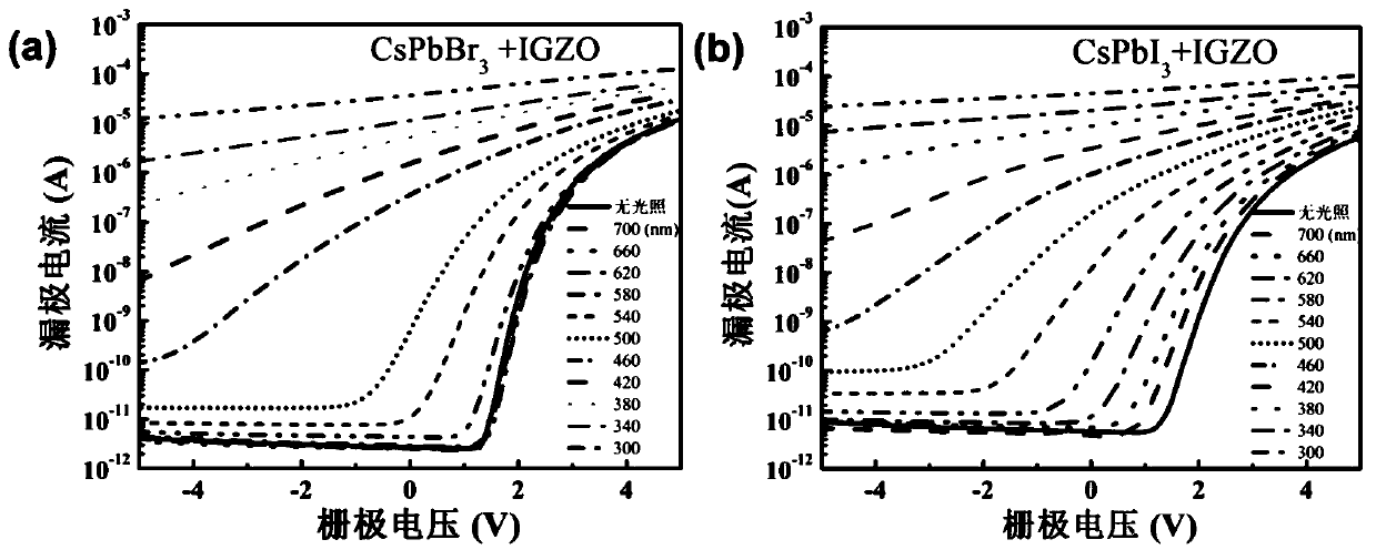
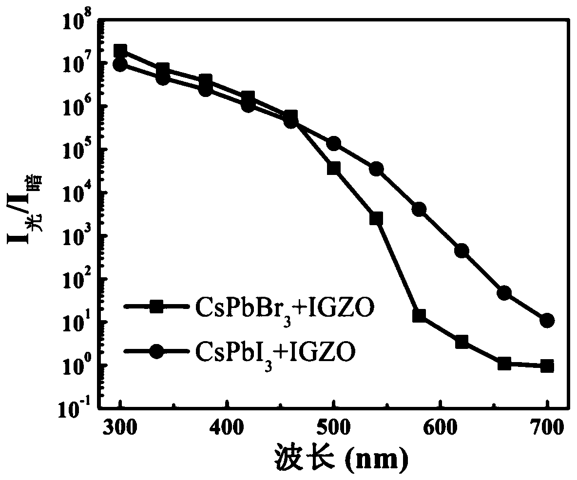
[0039] The photosensitive material used in this embodiment is CsPbBr 3 quantum dots.

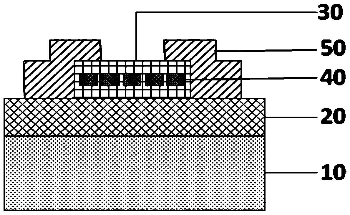
[0040] Such as figure 1 As shown, the photosensitive thin film transistor provided by the present invention has a structure from bottom to top: back gate electrode 10, gate dielectric layer 20, conductive channel 30, and source and drain electrodes 50, wherein perovskite quantum dots 40 are used as photosensitive materials , located in the middle of the conducting channel. Concrete preparation process is as follows:

[0041] (1) The back gate electrode 10 is made of heavily doped p-type silicon with a resistivity of <0.005 Ω•cm, and is cleaned with acetone, isopropanol, and deionized water in sequence before use.

[0042] (2) The gate dielectric layer 20 is made of Al 2 o 3 Thin film, oxygen source is oxygen plasma, aluminum source is trimethylaluminum (TMA), TMA temperature, oxygen gas flow rate and plasma generation power are set to 18 ℃, 150 sccm and 2500 W, respectively, growth tem...

Embodiment 2

[0047] The photosensitive material that present embodiment adopts is CsPbI 3 quantum dots. The specific preparation process is:

[0048] (1) The back gate electrode 10 is made of heavily doped p-type silicon with a resistivity of <0.005 Ω•cm, and is cleaned with acetone, isopropanol, and deionized water in sequence before use.

[0049] (2) The gate dielectric layer 20 is made of Al 2 o 3 For thin films, the oxygen source is oxygen plasma, the aluminum source is TMA, the TMA temperature, oxygen gas flow rate and plasma generation power are set to 18 ℃, 150 sccm and 2500 W, respectively, the growth temperature is 30 ℃, and the growth thickness is 40 nm.

[0050] (3) The conductive channel 30 is an amorphous IGZO film prepared by magnetron sputtering. The selected target is an IGZO target with an atomic ratio of In:Ga:Zn:O = 1:1:1:4. The total growth The thickness was 40 nm, and the working pressure, RF power, argon and oxygen gas flows were set to 0.88 Pa, 110 W, 48 and 2 sc...


PUM

PropertyMeasurementUnit
thicknessaaaaaaaaaa
thicknessaaaaaaaaaa

Abstract

The invention belongs to the technical field of semiconductor devices, and particularly relates to a photosensitive thin film transistor and a low-temperature preparation method thereof. According tothe photosensitive thin film transistor, perovskite quantum dots are adopted as a photosensitive material, and the device can respond to light with different wavelengths by changing the proportion ofhalogen elements in the perovskite quantum dots; and the preparation method of the photosensitive thin film transistor comprises the steps of preparing an Al2O3 gate dielectric through atomic layer deposition, growing an amorphous indium gallium zinc oxide (a-IGZO) channel layer through magnetron sputtering, preparing the perovskite quantum dots through adoption of a spin-coating method, and preparing source and drain electrodes through electron beam evaporation. The long temperature of all processes does not exceed 40 DEG C, and the high-performance photosensitive thin film transistor can beobtained without heat treatment in the device preparation process. The photosensitive thin film transistor and the low-temperature preparation method thereof can be applied to the fields of flexible electronics, photoelectric detection and the like.

Description

technical field [0001] The invention belongs to the technical field of semiconductor devices, and in particular relates to a photosensitive thin film transistor and a low-temperature preparation method thereof. Background technique [0002] Photodetectors are mainly composed of photosensitive elements. According to the different band gaps of photosensitive materials, photodetectors can detect ultraviolet, infrared and visible light. The photosensitive material in the ultraviolet detector is mainly a wide bandgap semiconductor, which can be applied to ultraviolet flame monitoring, material curing, sterilization and disinfection, etc. [1, 2]. Infrared detectors mainly use PbS, doped Si, Ge and Hg 1-x Cd x Te and other materials, and have been maturely applied in missile guidance and other aspects [3-5]. The materials used in visible light detectors mainly include CdS, CdSe, Si, Ge, etc., which can be applied to ray measurement, industrial automatic control, photometric meas...

Claims


Application Information

Patent Timeline
Patent Type & Authority Applications(China)
IPC IPC(8): H01L31/113H01L31/032H01L31/18
CPCH01L31/1136H01L31/032H01L31/18Y02P70/50
Inventor 丁士进王晓琳吴小晗张卫
Owner FUDAN UNIV
Why Eureka
Try Eureka