Test method of CMOS image sensor, and device

A technology of image sensor and testing method, which is applied in image communication, television, electrical components, etc., and can solve the problem of low efficiency of CMOS image sensor

Active Publication Date: 2020-04-14
JACAL ELECTRONICS WUXI
View PDF7 Cites 0 Cited by
  • Summary
  • Abstract
  • Description
  • Claims
  • Application Information

AI Technical Summary

Problems solved by technology

[0003] In order to solve the above-mentioned technical problems, the present invention provides a CMOS image sensor testing method and device to solve the problem of low efficiency of CMOS image sensor testing in the prior art, reduce the degree of manual participation, improve the degree of automation, and improve the efficiency of testing. efficiency

Method used


Image

  • Test method of CMOS image sensor, and device
  • Test method of CMOS image sensor, and device

Examples


Embodiment 1

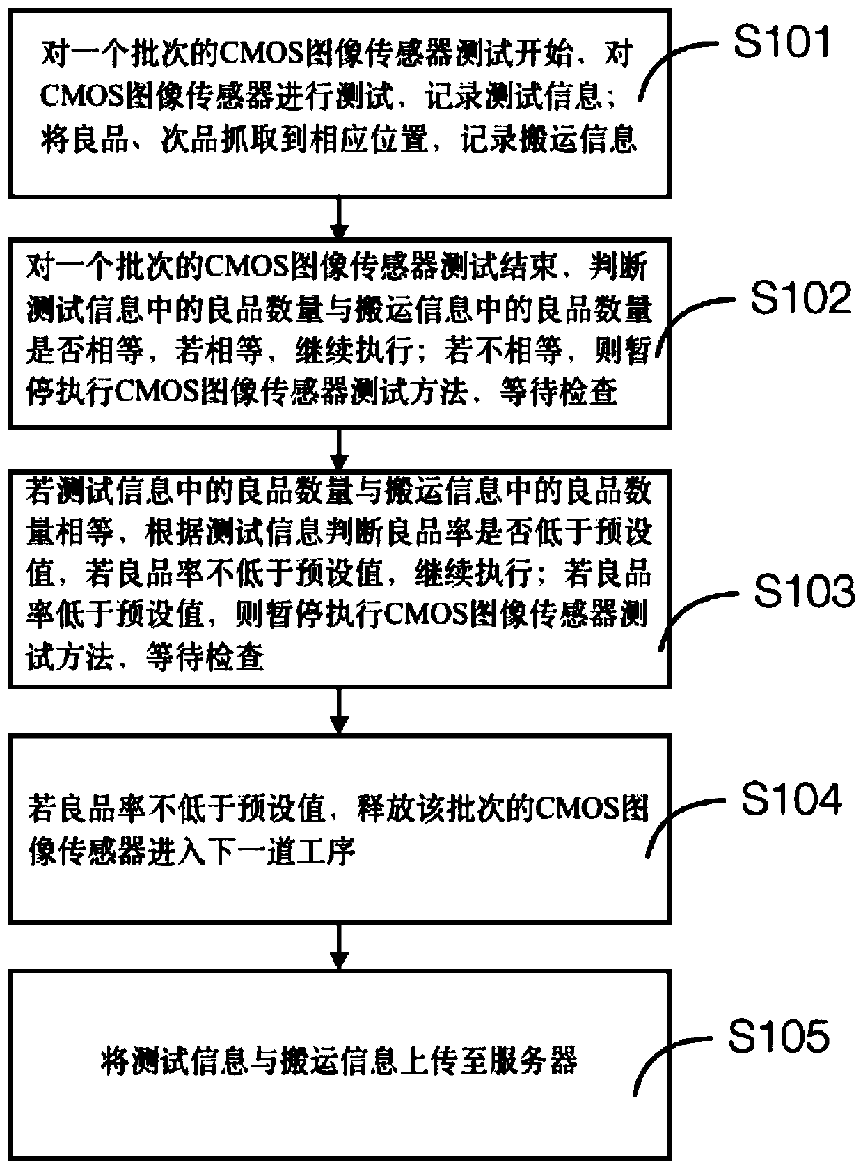
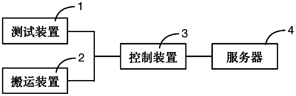
[0021] like figure 2 As shown, the test device for the CMOS image sensor provided in Embodiment 1 of the present invention includes a test device 1, a handling device 2, and a control device 3 (in this field, the test device is generally referred to as a tester, and the handling device is referred to as a handler for short). During the test process, the automatic comparison of the number of good products and the automatic judgment of good products are realized by controlling the work of the test device and the handling device, reducing the degree of manual participation, improving the degree of automation, and improving test efficiency; for the convenience of implementation, a CMOS is provided in this embodiment 1 Test methods for image sensors such as figure 1 shown, including:


PUM


Abstract

The invention provides a test method of a CMOS image sensor, and relates to an image sensor test, which comprises the following steps: ending the test of a batch of CMOS image sensors, judging whetherthe number of good products in test information is equal to the number of good products in carrying information or not, and continuing to execute if the number of good products is equal to the numberof good products in carrying information; if not, pausing to execute the CMOS image sensor test method, and waiting for inspection; if the number of the good products in the test information is equalto the number of the good products in the carrying information, judging whether the yield is lower than a preset value according to the test information, and if the yield is not lower than the presetvalue, continuing execution; if the yield is lower than the preset value, pausing to execute the CMOS image sensor test method, and waiting for inspection; and if the yield is not lower than the preset value, releasing the batch of CMOS image sensors to enter the next process. According to the method, the problem of low testing efficiency of the CMOS image sensor in the prior art is effectively solved, the automation of yield comparison and yield judgment is realized, the manpower is liberated, and the testing efficiency is improved.

Description

technical field [0001] The invention relates to image sensor testing, in particular to a CMOS image sensor testing method and device. Background technique [0002] The performance parameters of CMOS image sensors are generally evaluated and measured by the manufacturer during design and production, and typical values ​​are given. However, due to changes in the production process and semiconductor materials, the actual performance parameters of the image sensor used by the user may differ from the typical values ​​given. There are certain discrepancies, so the manufacturer needs to test the CMOS image sensor, and compare the number of good products after the test with the total amount of the test to determine whether the batch is qualified. In the existing test, it is necessary to manually check whether the number of good products picked up by the handling device after the test is consistent with the number of good products in the test; at the same time, it is necessary to ma...

Claims


Application Information

Patent Timeline
Patent Type & Authority Applications(China)
IPC IPC(8): H04N17/00
CPCH04N17/00
Inventor 王国建谭磊
Owner JACAL ELECTRONICS WUXI
Why Eureka
Try Eureka