Wafer cleaning and drying device

A drying device and wafer technology, which is applied in the manufacture of electrical components, circuits, semiconductor/solid-state devices, etc., can solve the problems of excessive particle quantity and water residue on the whole wafer, so as to improve the utilization rate and reduce water stains. Residual, avoid the effect of excessive quantity

Active Publication Date: 2020-07-14
HANGZHOU ZHONGGUI ELECTRONICS TECH CO LTD
View PDF7 Cites 5 Cited by
  • Summary
  • Abstract
  • Description
  • Claims
  • Application Information

AI Technical Summary

Problems solved by technology

However, due to the difference in the material of the wafer itself and the influence of the surface texture pattern, water stains will remain, and the amount of particulate matter in the entire wafer will exceed the standard

Method used


Image

  • Wafer cleaning and drying device
  • Wafer cleaning and drying device
  • Wafer cleaning and drying device

Examples


Embodiment Construction

[0031] The following will clearly and completely describe the technical solutions in the embodiments of the present invention with reference to the accompanying drawings in the embodiments of the present invention. Obviously, the described embodiments are only some, not all, embodiments of the present invention. Based on the embodiments of the present invention, all other embodiments obtained by persons of ordinary skill in the art without making creative efforts belong to the protection scope of the present invention.

[0032] The core of the present invention is to provide a wafer cleaning and drying device, which can effectively remove water stains on the surface of the wafer and prevent the particle quantity of the entire wafer from exceeding the standard.

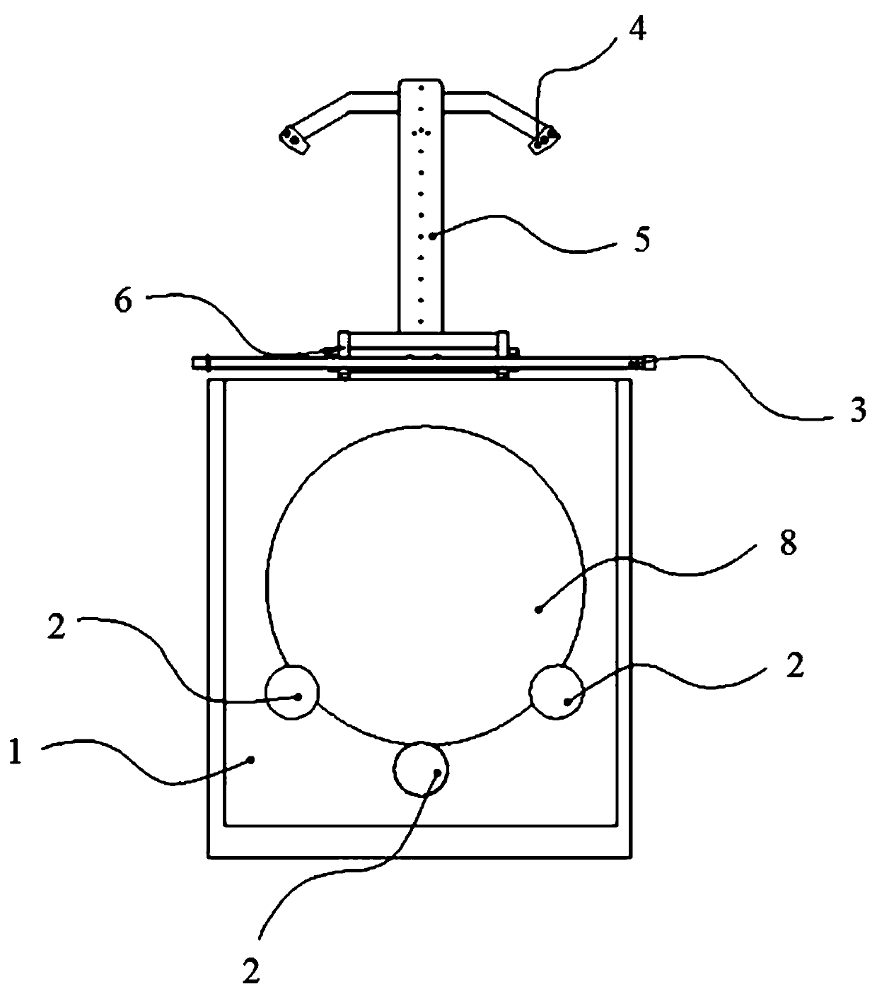
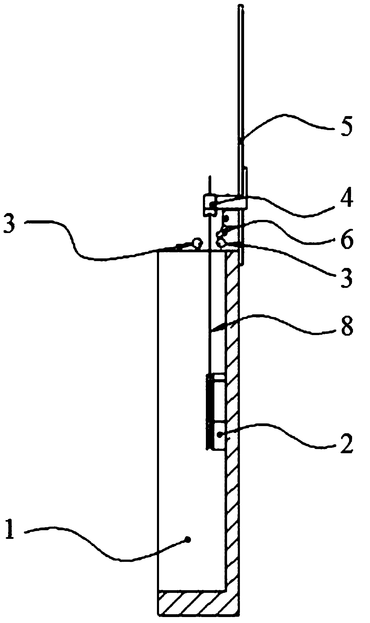
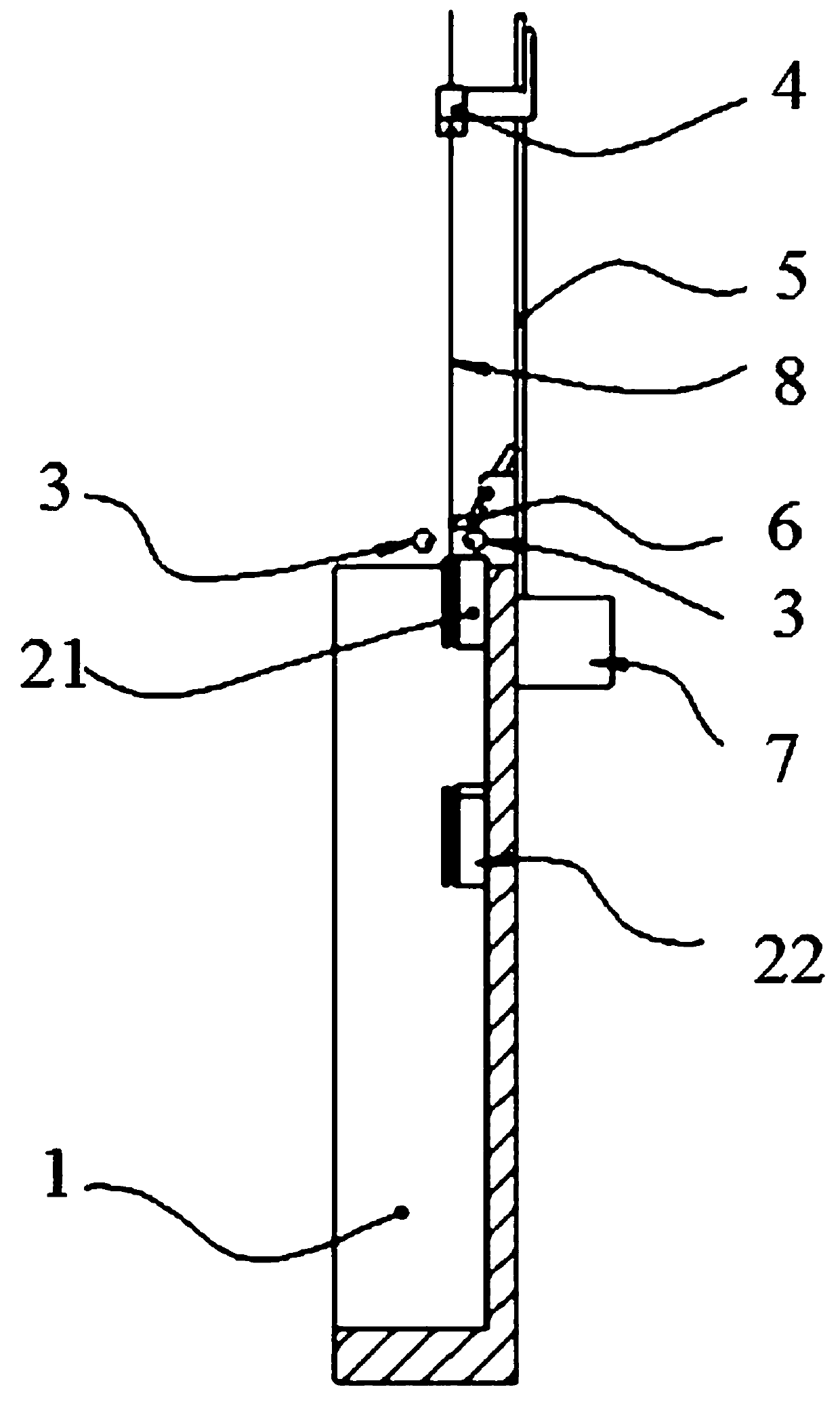
[0033] Please refer to Figure 1-Figure 5 , figure 1 The front view of the wafer cleaning and drying device provided for the specific embodiment of the present invention during wafer cleaning (the front side wall of t...


PUM


Abstract

The invention discloses a wafer cleaning and drying device, which comprises: a box body for cleaning the wafer, the top of the box body is provided with an opening for the wafer to enter and exit the box body; A support mechanism for accepting wafers, the support mechanism can be raised and lowered; a spray pipe arranged at the opening and used for spraying dry gas on the surface of the cleaned wafer. In the wafer cleaning and drying device, a spray pipe is arranged at the opening of the box, and the spray pipe is used to spray drying gas on the cleaned wafer to dry the surface of the wafer. It can be understood that this method utilizes the Marangoni effect, that is, the surface tension gradient is used to remove the water attached to the wafer surface. Compared with the cleaning solution that uses centrifugal force to dry the wafer surface in the prior art, The wafer cleaning and drying device can effectively reduce the residue of water stains and prevent the particle quantity of the entire wafer from exceeding the standard.

Description

technical field [0001] The invention relates to the technical field of semiconductor process equipment, and more specifically, to a wafer cleaning and drying device. Background technique [0002] In the manufacturing process of semiconductor integrated circuit chips, it is necessary to perform chemical mechanical planarization processing on the wafer, that is, to use a large amount of grinding liquid and different chemical reagents to polish the wafer surface. This chemical mechanical planarization process belongs to In the wet process, at the end of the process, the wafer needs to be cleaned and dried to remove particles attached to the wafer surface. [0003] In the prior art, the surface of the wafer is usually dried by spinning and drying, so as to remove the cleaning solution on the surface of the wafer by utilizing the centrifugal force generated when the wafer rotates at a high speed. However, due to the difference in the material of the wafer itself and the influenc...

Claims


Application Information

Patent Timeline
Patent Type & Authority Patents(China)
IPC IPC(8): H01L21/67H01L21/687
CPCH01L21/67034H01L21/67057H01L21/68792H01L21/67751H01L21/67742
Inventor 沈凌寒
Owner HANGZHOU ZHONGGUI ELECTRONICS TECH CO LTD
Why Eureka
Try Eureka