
Display device

A display device and display area technology, which is applied in the direction of instruments, electrical components, circuits, etc., can solve problems such as inaccuracy, touch failure of fingerprint recognition modules, etc.

Inactive Publication Date: 2020-05-05
WUHAN CHINA STAR OPTOELECTRONICS SEMICON DISPLAY TECH CO LTD
View PDF7 Cites 14 Cited by
  • Summary
  • Abstract
  • Description
  • Claims
  • Application Information

AI Technical Summary

Problems solved by technology

[0004] In order to solve the above technical problems, the present invention provides a display device to solve the technical problem in the prior art that the fingerprint recognition module is easily affected by non-touch light and causes touch failure or inaccuracy

Method used


Image

  • Display device
  • Display device
  • Display device

Examples


Embodiment 1

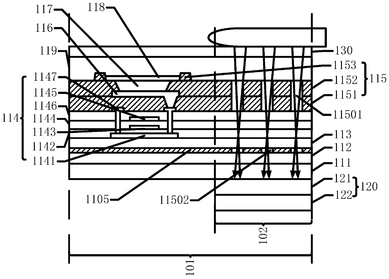
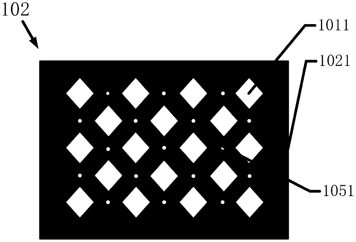
[0041] In this embodiment, the display device 10 of the present invention includes a display area 101 and a fingerprint identification area 102 disposed in the display area 101 .

[0042] The display area 101 further includes several pixel areas 1011 and light-shielding areas 1012 , the pixel areas 1011 are uniformly distributed in the display area 101 , and the light-shielding areas 1012 surround the pixel areas 1011 .

[0043] Such as figure 1 As shown, the display device 10 further includes a display panel 110 , a fingerprint identification group 120 and a touch layer 130 .

[0044] Such as figure 2 As shown, the display panel 110 includes a substrate 111 , a barrier layer 112 , a buffer layer 113 , a thin film transistor structure layer 114 , a light shielding structure 115 , an anode layer 116 , a light emitting layer 117 , a cathode layer 118 and an encapsulation layer 119 .

[0045] The barrier layer 112 is disposed on the substrate 111 to prevent external water vapo...


PUM


Abstract

The invention discloses a display device. The display device comprises a display area and a fingerprint identification area arranged in the display area, and further comprises a display panel which isprovided with a shading structure. In the fingerprint identification area, a plurality of light transmitting holes are formed in the shading structure. The display device further comprises a fingerprint identification group which is arranged below the display panel and corresponds to the fingerprint identification area. The display device has the beneficial effects that the materials of a flat layer, a pixel limiting layer and the retaining wall structure are changed into lightproof materials from light-transmitting materials in the prior art; the light transmitting holes are formed in the fingerprint identification area, so that non-touch effective light is prevented from influencing the precision of the fingerprint identification module; the accuracy of fingerprint identification and touch is improved; and the design of the light transmitting holes plays a role of a collimator, so that a collimator device in the fingerprint identification module can be removed, and the thickness ofthe display device is reduced.

Description

technical field [0001] The invention relates to the display field, in particular to a display device. Background technique [0002] As display terminal devices such as tablets enter the era of full screens, the fingerprint recognition area on the front of the display terminal is squeezed by the full screen, so the under-display or under-screen fingerprint recognition technology has attracted more and more attention. The fingerprint recognition technology under the screen refers to installing the fingerprint recognition module (such as the fingerprint recognition module) under the display screen, so as to realize the fingerprint recognition operation in the display area of ​​the display screen. Area Set the fingerprint collection area. [0003] Optical under-screen fingerprint recognition technology uses light returning from the top surface of the device's display assembly for fingerprint sensing and other sensing operations. The returned light carries information of an obj...

Claims


Application Information

Patent Timeline
IPC IPC(8): H01L27/32G06K9/00
CPCG06V40/1318H10K59/40H10K59/65H10K59/12H01L27/14623H10K59/8792H10K59/122G06V40/1365G06V40/1329G06V40/1324
Inventor 李远航
Owner WUHAN CHINA STAR OPTOELECTRONICS SEMICON DISPLAY TECH CO LTD
Learn More