Preparation and modulation method of photoelectric synaptic device

A technology of a synaptic device and a modulation method, applied in the field of artificial neural network, can solve the problems of limited optical band range, difficult to meet complex application scenarios, etc., and achieve the effect of widening the response range of optical waves

Active Publication Date: 2020-05-22
TIANJIN UNIVERSITY OF TECHNOLOGY
View PDF6 Cites 6 Cited by
  • Summary
  • Abstract
  • Description
  • Claims
  • Application Information

AI Technical Summary

Problems solved by technology

However, the current photoelectric synapse device simply integrates the photoelectric response function into the synapse device, and the range of light wavelengths it responds to is extremely limited, making it difficult to meet the requirements of complex application scenarios.

Method used


Image

  • Preparation and modulation method of photoelectric synaptic device
  • Preparation and modulation method of photoelectric synaptic device
  • Preparation and modulation method of photoelectric synaptic device

Examples


Embodiment Construction

[0041] The present invention will be further described in detail below in conjunction with the accompanying drawings and specific embodiments. For the step numbers in the following embodiments, it is only set for the convenience of illustration and description, and the order between the steps is not limited in any way. The execution order of each step in the embodiments can be adapted according to the understanding of those skilled in the art sexual adjustment.

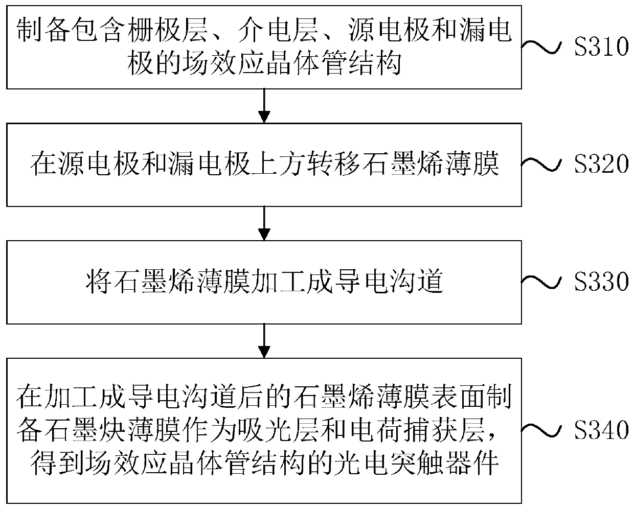
[0042] refer to figure 1 , the embodiment of the present invention provides a method for preparing a photoelectric synapse device, which includes the following steps:

[0043] S310, preparing a field effect transistor structure including a gate layer, a dielectric layer, a source electrode and a drain electrode;

[0044] S320, transferring the graphene film over the source electrode and the drain electrode;

[0045] S330, processing the graphene film into a conductive channel;

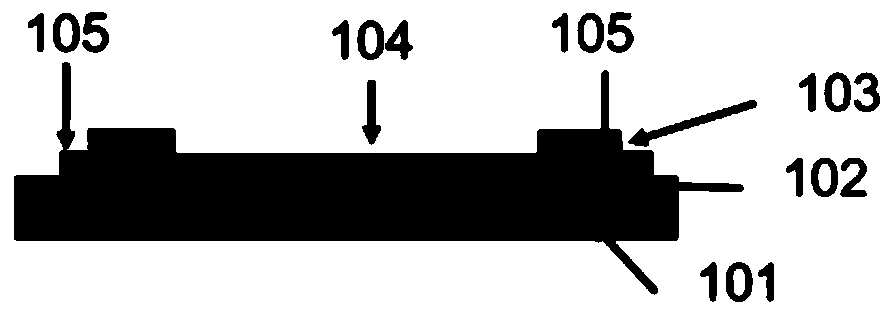
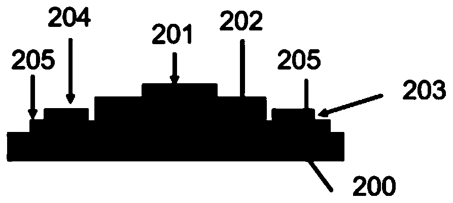
[0046] S340, preparing a graphene f...


PUM

PropertyMeasurementUnit
wavelengthaaaaaaaaaa

Abstract

The invention discloses a preparation and modulation method of a photoelectric synaptic device. The preparation method comprises the following steps: preparing a field effect transistor structure comprising a gate layer, a dielectric layer, a source electrode and a drain electrode; transferring a graphene thin film over the source electrode and the drain electrode; processing the graphene film into a conductive channel; and preparing a graphdiyne thin film on the surface of the graphene thin film processed into the conductive channel to obtain the photoelectric synapse device of the field effect transistor structure. According to the invention, the graphene film is transferred above the source electrode and the drain electrode, the graphdiyne thin film is prepared on the surface of the graphene thin film to obtain the photoelectric synapse device of the field effect transistor structure, by preparing the graphdiyne thin film on the surface of the graphene thin film, the light wave response range is widened, regulation and control of light signals and electric signals are achieved through the field effect transistor structure, and therefore the requirements under complex applicationscenes are met. The method can be widely applied to the technical field of artificial neural networks.

Description

technical field [0001] The invention relates to the technical field of artificial neural networks, in particular to a method for preparing and modulating a photoelectric synapse device. Background technique [0002] Neuromorphic computing is one of the fastest-growing technologies in the past decade. It achieves efficient parallel processing of large amounts of data by simulating the edge computing of the human nervous system, and overcomes the problems caused by the separation of memory and processor in traditional von Neumann computers. Disadvantages such as computing delays and high energy consumption are of great significance for promoting the development of artificial intelligence, machine learning, autonomous driving and other fields. For artificial neural networks, a large amount of data needs to be obtained from the external environment with the help of various sensors, the most important of which is the visual sensor, and more than 80% of the information is obtained...

Claims


Application Information

Patent Timeline
Patent Type & Authority Applications(China)
IPC IPC(8): H01L31/18H01L31/028H01L31/113G06N3/067
CPCG06N3/0675H01L31/028H01L31/1136H01L31/1804Y02P70/50
Inventor 鲁统部王静静陈旭东张志成
Owner TIANJIN UNIVERSITY OF TECHNOLOGY
Why Eureka
Try Eureka