Fast recovery diode device structure and manufacturing method thereof

A technology for recovering diode and device structures, applied in semiconductor/solid-state device manufacturing, semiconductor devices, electrical components, etc., to achieve process compatibility and simple process control

Pending Publication Date: 2020-05-29
SHANGHAI DAOZHI TECH CO LTD
View PDF0 Cites 4 Cited by
  • Summary
  • Abstract
  • Description
  • Claims
  • Application Information

AI Technical Summary

Problems solved by technology

In the field of high frequency and high power, there is no other device that can replace it

Method used


Image

  • Fast recovery diode device structure and manufacturing method thereof
  • Fast recovery diode device structure and manufacturing method thereof
  • Fast recovery diode device structure and manufacturing method thereof

Examples


Embodiment Construction

[0024] In order to make those skilled in the art more clearly understand the purpose, technical solutions and advantages of the present invention, the present invention will be further described below in conjunction with the accompanying drawings and embodiments.

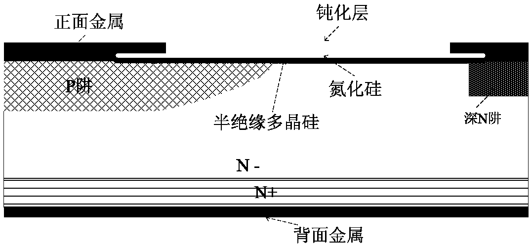
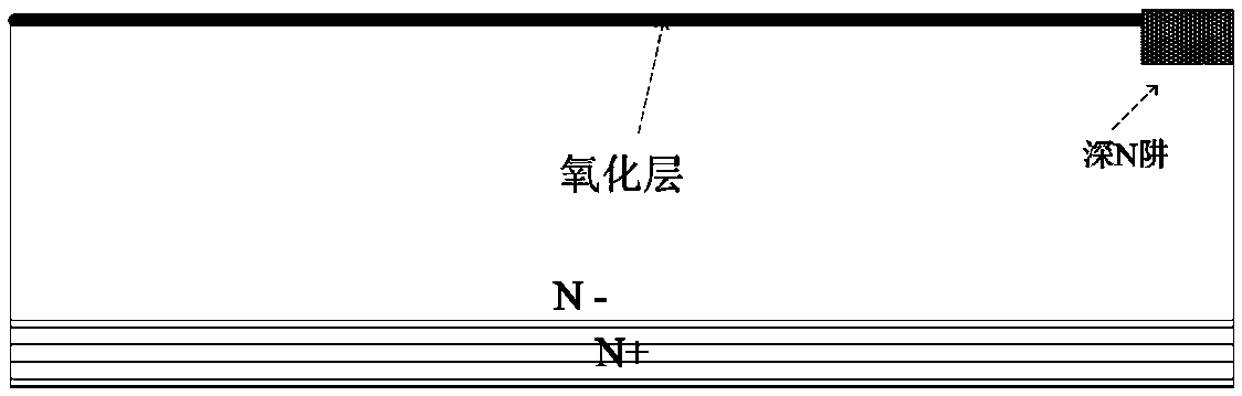
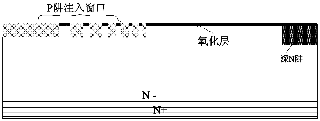
[0025] Such as Figure 1-5 As shown, a fast recovery diode device structure according to the present invention mainly includes an N-type epitaxial substrate, and the N-type epitaxial substrate includes an N+ substrate layer and an N- epitaxial layer arranged on the N+ substrate layer, A semi-insulating polysilicon layer and a silicon oxide layer are sequentially arranged in the middle of the top of the N-epitaxial layer, and a front metal layer is arranged on the left and right sides of the top of the N-epitaxial layer, and the height of the front metal layer is higher than that of the semi-insulating layer. The height of the polysilicon layer and the silicon oxide layer, the top of the silicon oxide layer and one s...


PUM


Abstract

The invention discloses a fast recovery diode device structure and a manufacturing method thereof. The structure mainly comprises an N+ substrate layer and an N- epitaxial layer arranged on the N+ substrate layer. A semi-insulating polycrystalline silicon layer and a silicon oxide layer are sequentially arranged in the middle of a top of the N- epitaxial layer; front metal layers are arranged on aleft side and a right side of a top of the N- epitaxial layer; and the front metal layers are higher than the semi-insulating polycrystalline silicon layer and the silicon oxide layer, passivation layers are arranged at the silicon oxide layer and a top of the front metal layer on one side, and a back metal layer is arranged at a bottom of the N+ substrate layer. The manufacturing method mainly comprises the steps of defining an active region and a growth field region oxide layer; depositing insulating materials such as semi-insulating polycrystalline silicon (SIPOS), silicon nitride and thelike after etching a silicon surface oxide layer, and annealing and densifying; photoetching a contact hole, etching an insulating layer, sputtering top metal, photoetching the top metal, depositing polyimide as the passivation layer, and photoetching the passivation layer; and finally carrying out a minority carrier lifetime control process to form a diode with a rapid recovery characteristic.

Description

technical field [0001] The invention belongs to the technical field of semiconductor device manufacturing, and in particular relates to a fast recovery diode device structure and a manufacturing method thereof. Background technique [0002] Whether the main circuit in the modern power electronic circuit is a thyristor with commutation shutdown or a new type of power electronic device with self-shutdown capability, such as GTO, MOSFET, IGBT, etc., it needs a power fast recovery diode connected in parallel. , to pass the reactive current in the load, reduce the charging time of the main switching device capacitor, and at the same time suppress the high voltage induced by the parasitic inductance when the load current reverses instantaneously. As the main representative of new power semiconductor devices, IGBT modules are widely used in the fields of industry, information, new energy, medicine, transportation, military and aviation. At present, the withstand voltage of IGBT mo...

Claims


Application Information

Patent Timeline
Patent Type & Authority Applications(China)
IPC IPC(8): H01L29/868H01L21/329
CPCH01L29/6609H01L29/868
Inventor 伽亚帕·维拉玛·苏巴斯沈华永福周旭明
Owner SHANGHAI DAOZHI TECH CO LTD
Why Eureka
Try Eureka