Method of forming oxide film on an SOI layer and method of fabricating a bonded wafer

a technology of oxide film and soi layer, which is applied in the direction of basic electric elements, electrical apparatus, semiconductor devices, etc., can solve the problems of manysimox methods, limited thickness and thickness uniformity of the resultant soi layer, and slight damage to the surface of the soi layer, etc., to achieve excellent crystallinity, prevent crystal defects, and high degree of thickness uniformity

Inactive Publication Date: 2001-05-29
SHIN-ETSU HANDOTAI CO LTD
View PDF11 Cites 29 Cited by
  • Summary
  • Abstract
  • Description
  • Claims
  • Application Information

AI Technical Summary

Benefits of technology

As described above, the present invention is effective in preventing generation of crystal defects and the like in a very thin SOI layer having a thickness of 1 .mu.m or less, which has been recently demanded. That is, when an oxide film is formed on such a very thin SOI layer, a large stress acts on the SOI layer, so that crystal defects and the like are easily generated in the SOI layer. The present invention can prevent generation of such defects and the like.
The method of the present invention enables fabrication of a silicon bonded wafer, in which residual damage and crystal defects generated during the vapor-phase etching or the subsequent polishing have been reliably removed, and which therefore has a...

Problems solved by technology

However, the SIMOX method has many problems in relation to the reliability of a buried oxide film, the crystallinity of the SOI layer, and necessity of heat treatment at a temperature of 1300.degree. C. or higher.
However, since the thin film is formed by means of mechanical machining, there are limits in relation to the thickness and the thickness uniformity of the resultant SOI layer.
However, in the above-described PACE method, since the surface of a thin film is removed through use of RF plasma, slight damage is generated at the surface of an SOI layer.
That is, use of touch polishing does not eliminate damage and crystal defects generated during the process according to the PACE method, or the touch polishing itself generates...

Method used


Image

  • Method of forming oxide film on an SOI layer and method of fabricating a bonded wafer
  • Method of forming oxide film on an SOI layer and method of fabricating a bonded wafer
  • Method of forming oxide film on an SOI layer and method of fabricating a bonded wafer

Examples


Embodiment Construction

Next, the present invention will be described by way of example. However, the present invention is not limited thereto.

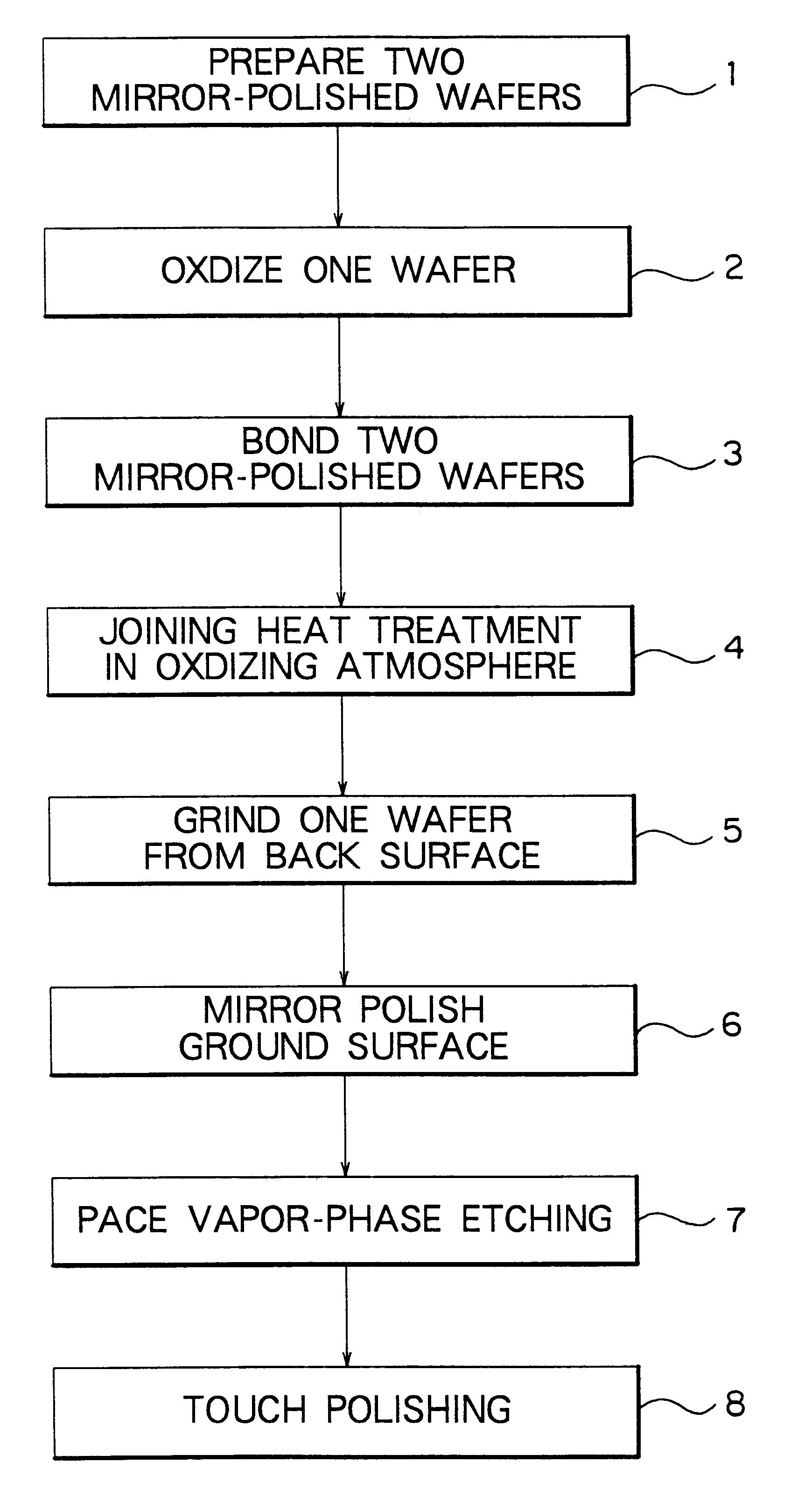
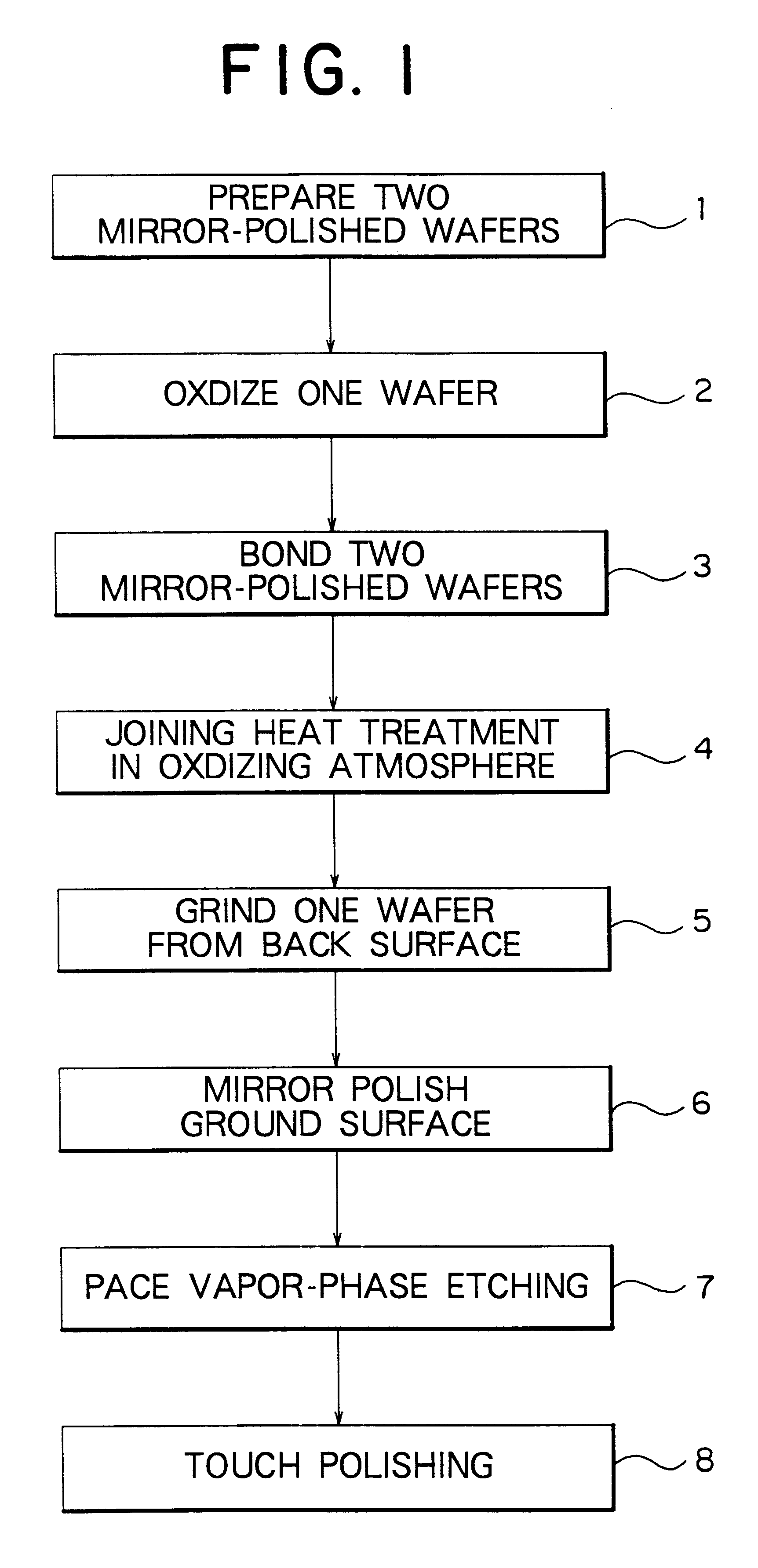
Twenty-four mirror-polished silicon wafers having a diameter of 150 mm (conductive type: p type; resistivity: 10 .OMEGA..multidot.cm) were prepared and divided into 12 bond wafers and 12 base wafers. These wafers were joined in accordance with the processes shown in FIG. 1 in order to yield 12 bonded wafers whose SOI layer had a thickness of 0.8 .mu.m. The 12 bonded wafers were subjected to thermal oxidation two pieces at a time such that the thickness of the oxide film became 6 nm, 24 nm, 50 nm, 110 nm, 275 nm, or 685 nm (six kinds). For the oxide film thicknesses of 6 nm, 24 nm, and 50 nm, an oxidation atmosphere containing 95% nitrogen and 5% oxygen was used. For the oxide film thicknesses of 110 nm, 275 nm, and 685 nm, a wet oxygen atmosphere was used. Subsequently, the oxide film was removed through use of aqueous solution of hydrofluoric acid, and then prefere...


PUM


Abstract

In a method of fabricating a bonded wafer, an oxide film is first formed on the surface of at least one of two mirror-polished silicon wafers. The two silicon wafers are superposed such that the mirror-polished surfaces come into close contact with each other, and heat treatment is performed in order to join the wafers together firmly. Subsequently, the thickness of one of the wafers is reduced so as to yield a thin film, the surface of which is then polished and subjected to vapor-phase etching in order to make the thickness of the thin film uniform. Optionally, the vapor-phase-etched surface is then mirror-polished. The surface of the bonded wafer is oxidized, and the generated surface oxide film is then removed. In the method, the thickness of the oxide film formed on the surface of the bonded wafer is made not greater than 50 nm. The method reliably eliminates damage and crystal defects generated during etching in accordance with PACE method or subsequent mirror polishing, and thereby enables relatively simple and low cost manufacture of bonded wafers having a very thin SOI layer that has good thickness uniformity and excellent crystallinity.

Description

1. Field of the InventionThe present invention relates to a technique for forming an oxide film on a wafer having an SOI (Silicon on Insulator) structure and to a technique for fabricating a bonded wafer having an SOI structure in which two mirror-polished silicon wafers are bonded together without use of adhesive, one of the wafers subsequently being made very thin.2. Description of the Related ArtTwo methods have been widely noticed as methods for fabricating wafers having an SOI structure. One method is a SIMOX (separation by implanted oxygen) method in which oxygen ions are implanted into a silicon monocrystal at a high concentration, and heat treatment is then performed at a high temperature in order to form an oxide film. The other method is a bonding method in which two mirror-polished silicon wafers are bonded together without use of adhesive, one of the wafers subsequently being made very thin.In the SIMOX method, the thickness of an SOI layer that becomes a device active r...

Claims


Application Information

Patent Timeline
IPC IPC(8): H01L21/70H01L21/762H01L21/02H01L21/20H01L21/304H01L27/12
CPCH01L21/2007H01L21/76251H01L21/02024H01L21/3247
Inventor AGA, HIROJIMITANI, KIYOSHINAKANO, MASATAKE
Owner SHIN-ETSU HANDOTAI CO LTD
Why Eureka
Try Eureka