
Bulk acoustic wave resonator, method for manufacturing bulk acoustic wave resonator, bulk acoustic wave resonator unit, filter, and electronic device

A technology of bulk acoustic wave resonators and resonators, applied in the direction of electrical components, impedance networks, etc., can solve the problems of low electromechanical coupling coefficient, high defect density, and poor piezoelectric characteristics of resonators

Pending Publication Date: 2020-06-05
TIANJIN UNIV +1
View PDF7 Cites 19 Cited by
  • Summary
  • Abstract
  • Description
  • Claims
  • Application Information

AI Technical Summary

Problems solved by technology

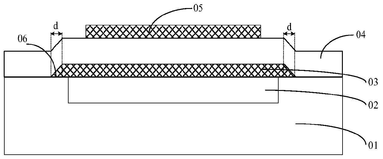
[0004] At present, most of the piezoelectric thin film materials used in traditional thin film bulk acoustic resonators are polycrystalline nitride thin films prepared by physical or chemical deposition techniques such as magnetron sputtering, and the piezoelectric properties are poor (mainly reflected in the low electromechanical coupling coefficient of the resonator. ), the defect density is high (mainly reflected in the low quality factor of the resonator), the heat dissipation is not good (mainly reflected in the low power capacity of the resonator), and there are etched oblique end faces at both ends of the bottom electrode of the resonator as shown in the figure As shown in 06 in 1, since the surface is generally rough, the defects in the piezoelectric layer deposited on the inclined end faces of the bottom electrode as shown in the region d in Figure 1 will be further enlarged
The existence of these defects will lead to acoustic loss, which will reduce the Q factor of the resonator, and cannot meet the technical indicators such as lower insertion loss and higher bandwidth required by future mobile communication technology.

Method used


Image

  • Bulk acoustic wave resonator, method for manufacturing bulk acoustic wave resonator, bulk acoustic wave resonator unit, filter, and electronic device
  • Bulk acoustic wave resonator, method for manufacturing bulk acoustic wave resonator, bulk acoustic wave resonator unit, filter, and electronic device
  • Bulk acoustic wave resonator, method for manufacturing bulk acoustic wave resonator, bulk acoustic wave resonator unit, filter, and electronic device

Examples


Embodiment Construction

[0032] The technical solutions of the present invention will be further specifically described below through the embodiments and in conjunction with the accompanying drawings. In the specification, the same or similar reference numerals designate the same or similar components. The following description of the embodiments of the present invention with reference to the accompanying drawings is intended to explain the general inventive concept of the present invention, but should not be construed as a limitation of the present invention. Some, but not all, embodiments of the invention. All other embodiments obtained by persons of ordinary skill in the art based on the embodiments of the present invention belong to the protection scope of the present invention.

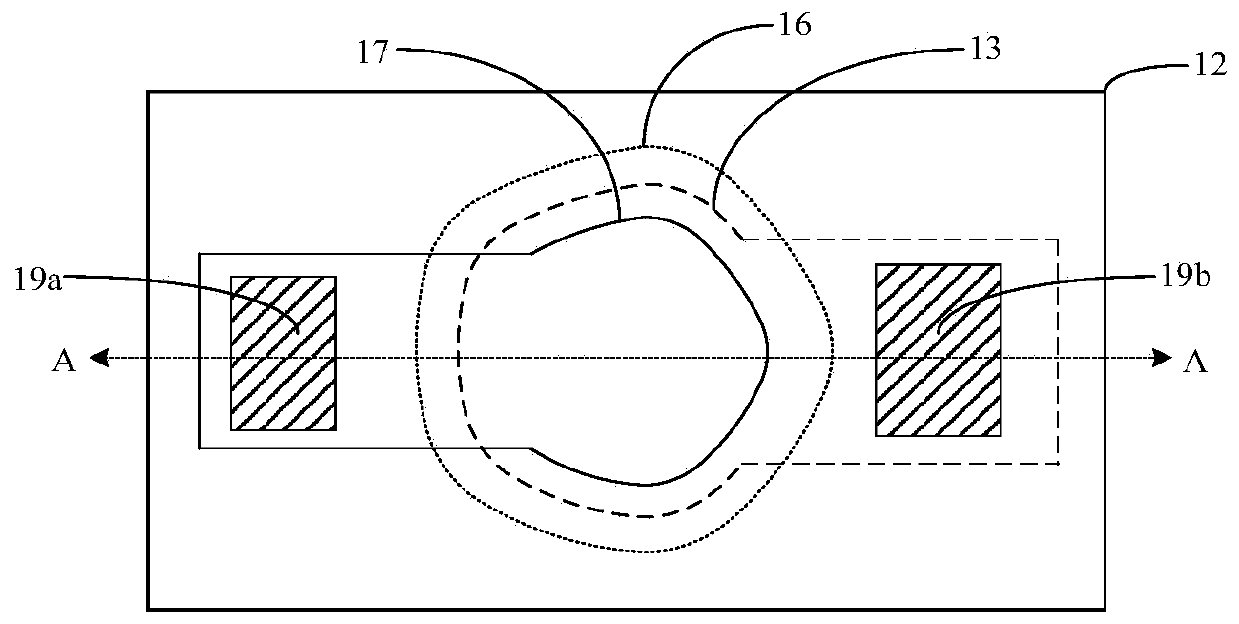
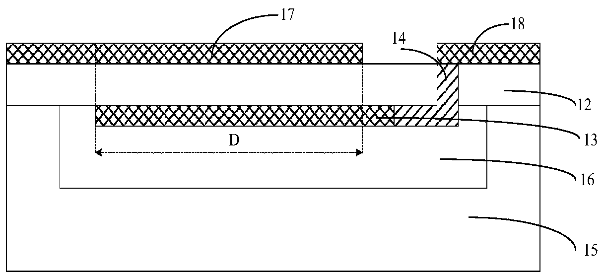
[0033] Figure 1B is a top view of a single crystal piezoelectric thin film bulk acoustic resonator according to an exemplary embodiment of the present invention. Among them, 16 is the air gap or cavity of the single ...


PUM


Abstract

The present invention relates to a single crystal thin film bulk acoustic resonator, comprising: a substrate; an acoustic mirror; a bottom electrode, connected with the bottom electrode pin; a top electrode, connected with the top electrode pin; a piezoelectric layer, arranged between the bottom electrode and the top electrode, wherein the piezoelectric layer is a single crystal film piezoelectriclayer, and an overlapping region of the acoustic mirror, the bottom electrode, the top electrode and the single crystal film piezoelectric layer in the thickness direction of the resonator forms an effective region of the resonator. The projections of the non-pin end of the top electrode and the non-pin end of the bottom electrode in the thickness direction of the resonator can be spaced apart from the edge of the acoustic mirror. The invention further relates to a manufacturing method of the single-crystal film bulk acoustic resonator, a single-crystal film bulk acoustic resonator unit withthe single-crystal film resonator and an electronic device.

Description

technical field [0001] Embodiments of the present invention relate to the field of semiconductors, and in particular to a bulk acoustic wave resonator, a filter with the resonator, a bulk acoustic wave resonator unit, and an electronic device with the resonator or the filter . Background technique [0002] With the increasing development of 5G communication technology, the requirements for communication frequency bands are getting higher and higher. Due to the limitation of structure and performance, traditional radio frequency filters cannot meet the requirements of high frequency communication. Film Bulk Acoustic Resonator (FBAR), as a new type of MEMS device, is well adapted to the upgrading of wireless communication systems, making FBAR technology one of the research hotspots in the field of communication. Compared with traditional bulk acoustic resonators, FBAR thin film bulk acoustic resonators, which have the advantages of small size, light weight, low insertion los...

Claims


Application Information

Patent Timeline
IPC IPC(8): H03H9/17H03H9/02H03H3/02H03H9/54
CPCH03H9/171H03H9/02007H03H3/02H03H9/54H03H2003/023H03H9/02118H03H9/173H03H9/0523H03H9/105H03H2003/021H03H9/174H03H9/0561
Inventor 张孟伦庞慰杨清瑞
Owner TIANJIN UNIV
Learn More