Eureka AIR delivers breakthrough ideas for toughest innovation challenges, trusted by R&D personnel around the world.

Three dimensional composite circuit board

A combined circuit and circuit board technology, applied in the direction of printed circuit, multilayer circuit manufacturing, printed circuit components, etc., can solve the problems of malfunction, difficult miniaturization of equipment, harm to users, etc., to reduce malfunction, reduce size, The effect of reducing waste

Inactive Publication Date: 2003-06-25
SAMSUNG ELECTRONICS CO LTD
View PDF1 Cites 0 Cited by
  • Summary
  • Abstract
  • Description
  • Claims
  • Application Information

AI Technical Summary

Problems solved by technology

[0006] However, it is difficult to manufacture a flexible circuit board with a multilayer structure
In addition, a large space is required in the device for mounting a multilayer flexible circuit board, making it difficult to miniaturize the device
Moreover, since the flexible circuit board has a multi-sided shape, even if one of the multi-sided surfaces fails, the circuit boards constituting the other sides cannot be used.
[0007] In addition, fixing the flexible circuit board in the equipment not only requires a fixing device, but also the electromagnetic waves generated by the electronic components of the flexible circuit board are not shielded, so that the electromagnetic waves cause malfunction of the equipment and may harm the user

Method used


Image

  • Three dimensional composite circuit board
  • Three dimensional composite circuit board
  • Three dimensional composite circuit board

Examples


Embodiment Construction

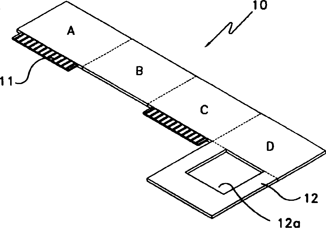
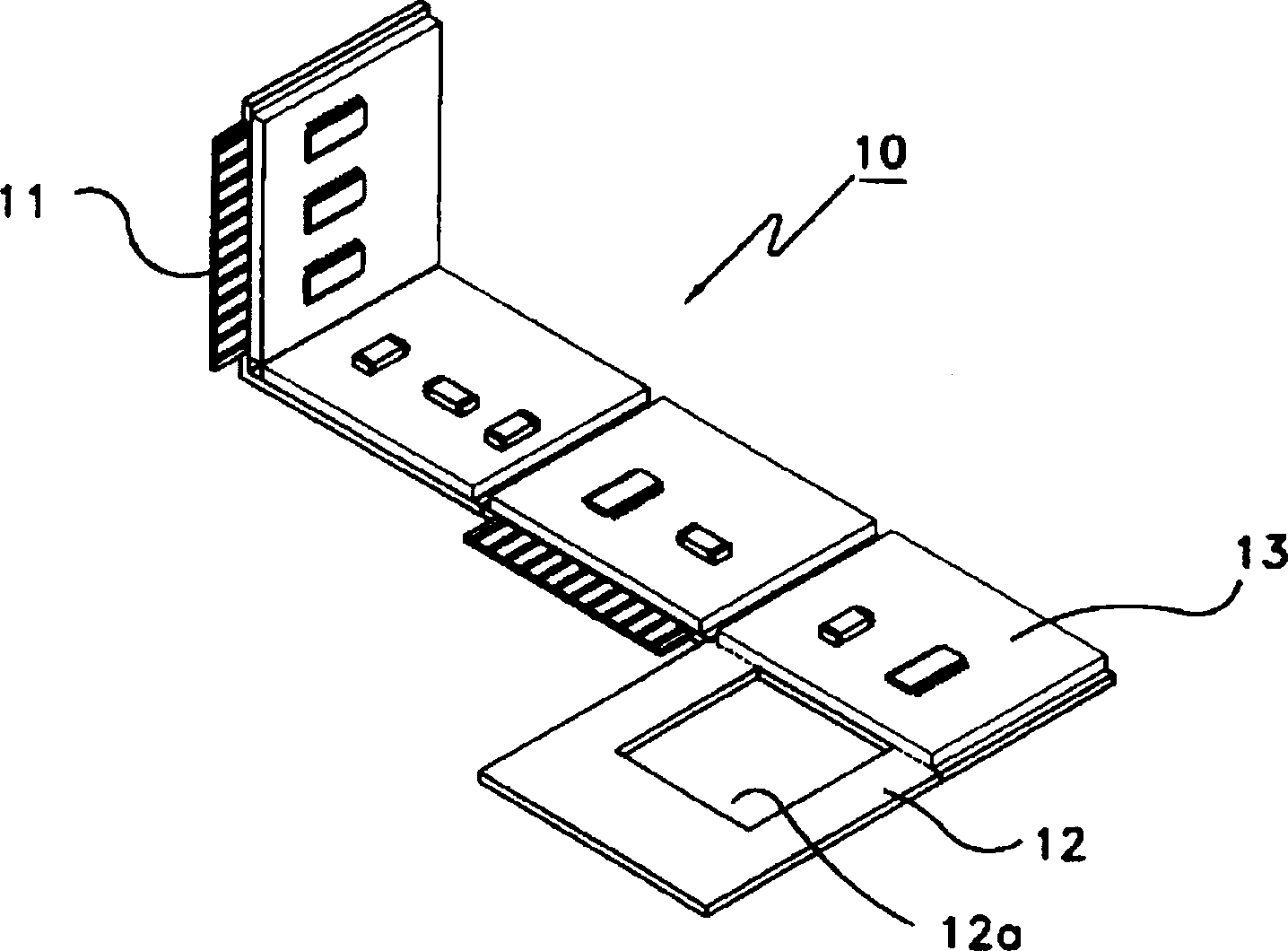
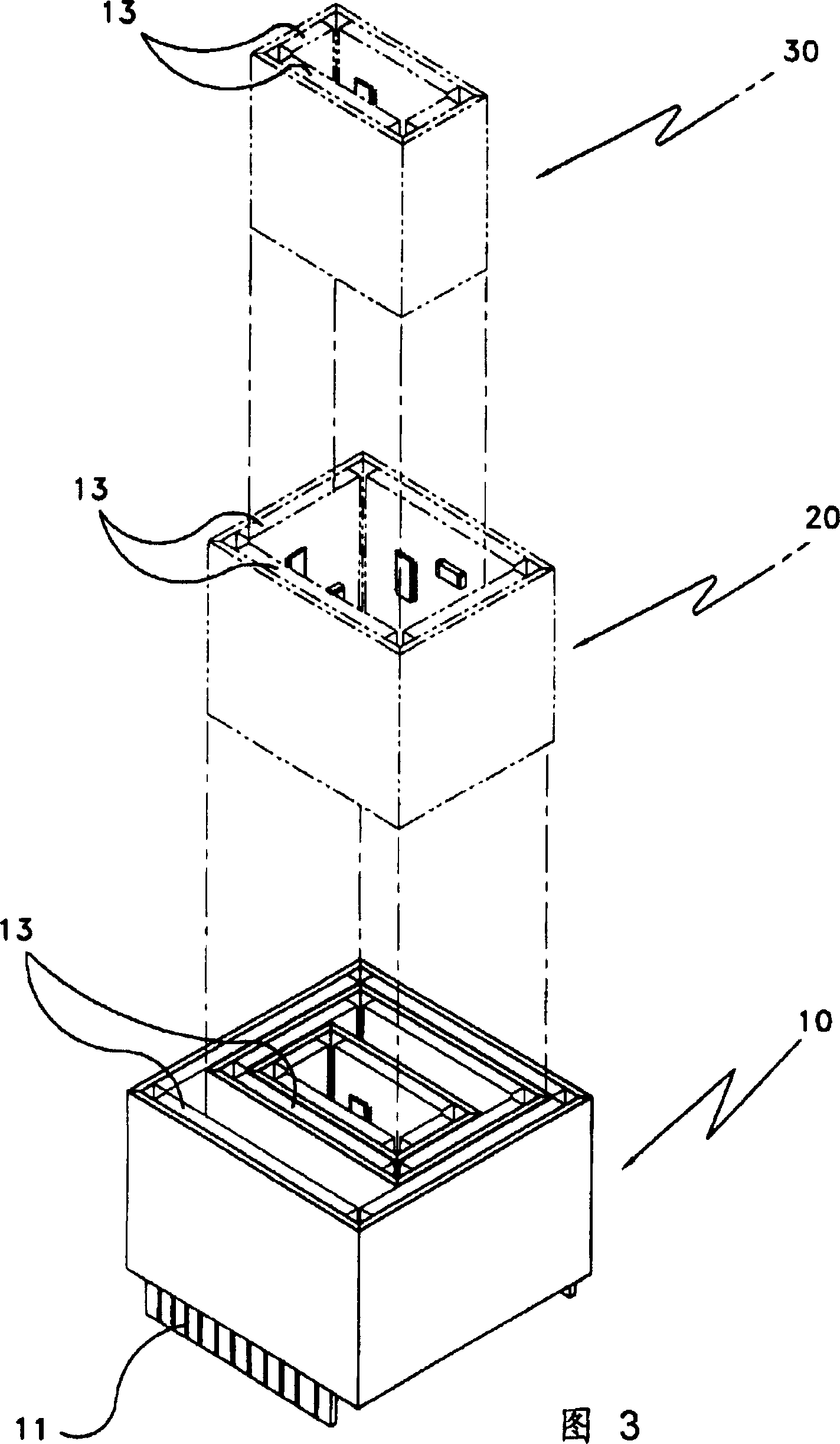
[0031] figure 1 - Figure 4 represents a three-dimensional composite circuit board according to the invention. This three-dimensional combined circuit board is made of the first circuit board 10, which is formed into a plate shape by plastic injection molding. The first circuit board 10 has 3 curved portions, thereby having a box shape. When it is unfolded, the first circuit board 10 is divided into A, B, C and D board sections having the same size. A fixing portion 11 protrudes from one side of the A and C board portions for fixing the first circuit board 10 to an electronic device.

[0032] At least one of the B and D board portions has a bottom plate 12 including an opening 12a, and a plurality of electronic components are mounted inside the A-D board portions. In order to shield electromagnetic waves generated by the electronic components, the first circuit board 10 is covered by the molding material 13 in such a manner that the electronic components and brazed portions ...


PUM


Abstract

A three dimensional composite circuit board includes a first, second, and third circuit boards and a molding material. The first, second and third circuit board have a plurality of plates which are each folded in order to form a separate cubic shape. The second circuit board has a volume smaller than a volume of the first circuit board so as to be accommodated in the first circuit board, and is coupled to the first circuit board. The third circuit board has a volume smaller than the volume of the second circuit board so as to be accommodated in the second circuit board, and is coupled to the second circuit board. The molding material coats electronic elements which are mounted in the first, second and third circuit boards and brazing portions of the electronic elements to shield the electromagnetic waves generated by the electronic elements.

Description

technical field [0001] The present invention relates to a three-dimensional built-up circuit board, and more particularly to a box-shaped built-up circuit board manufactured by assembling a circuit board with electronic components, whereby the size of a device including the circuit board is minimized. Background technique [0002] Generally speaking, circuit boards used in electrical, electronic or telecommunication equipment are made to have a planar shape. Such a circuit board is provided with a printed circuit pattern. In addition, various electronic components are systematically mounted on the circuit board according to the circuit pattern. [0003] When the board is installed in the equipment, the board is stacked in multiple layers. A separate device is required for mounting the circuit board in the device. [0004] However, such circuit boards are generally formed in two-dimensional shapes. Therefore, when a complicated circuit pattern is printed on a circuit boar...

Claims


Application Information

Patent Timeline
Patent Type & Authority Patents(China)
IPC IPC(8): H05K9/00H05K1/02H05K1/14H05K1/18H05K7/02
CPCH05K1/147H05K7/023H05K1/189H05K3/46
Inventor 张卿寓
Owner SAMSUNG ELECTRONICS CO LTD
Why Eureka
Eureka Blog
Learn More