Preparation method of display substrate, display substrate and display device

A technology for display substrates and display devices, which is used in semiconductor/solid-state device manufacturing, semiconductor devices, electrical components, etc., and can solve problems such as inability to integrate front cameras, infrared sensors, and inability to achieve full screen

Active Publication Date: 2020-06-16
BOE TECH GRP CO LTD +1
View PDF5 Cites 21 Cited by
  • Summary
  • Abstract
  • Description
  • Claims
  • Application Information

AI Technical Summary

Problems solved by technology

However, although the screens of display devices that have been mass-produced in related technologies are called full screens, they are actually "notch screens". Integrate optical components such as front camera and infrared sensor
Therefore, it is necessary to punch holes or set notch areas on the screen to integrate optical components so as to realize the functions of optical components in the display device. Therefore, in the current related technologies, only "notch screens" can be realized, and it is impossible to realize the "notch screen" in the true sense full screen

Method used


Image

  • Preparation method of display substrate, display substrate and display device
  • Preparation method of display substrate, display substrate and display device
  • Preparation method of display substrate, display substrate and display device

Examples


Embodiment Construction

[0039] In order to make the above objects, features and advantages of the present invention more comprehensible, the present invention will be further described in detail below in conjunction with the accompanying drawings and specific embodiments.

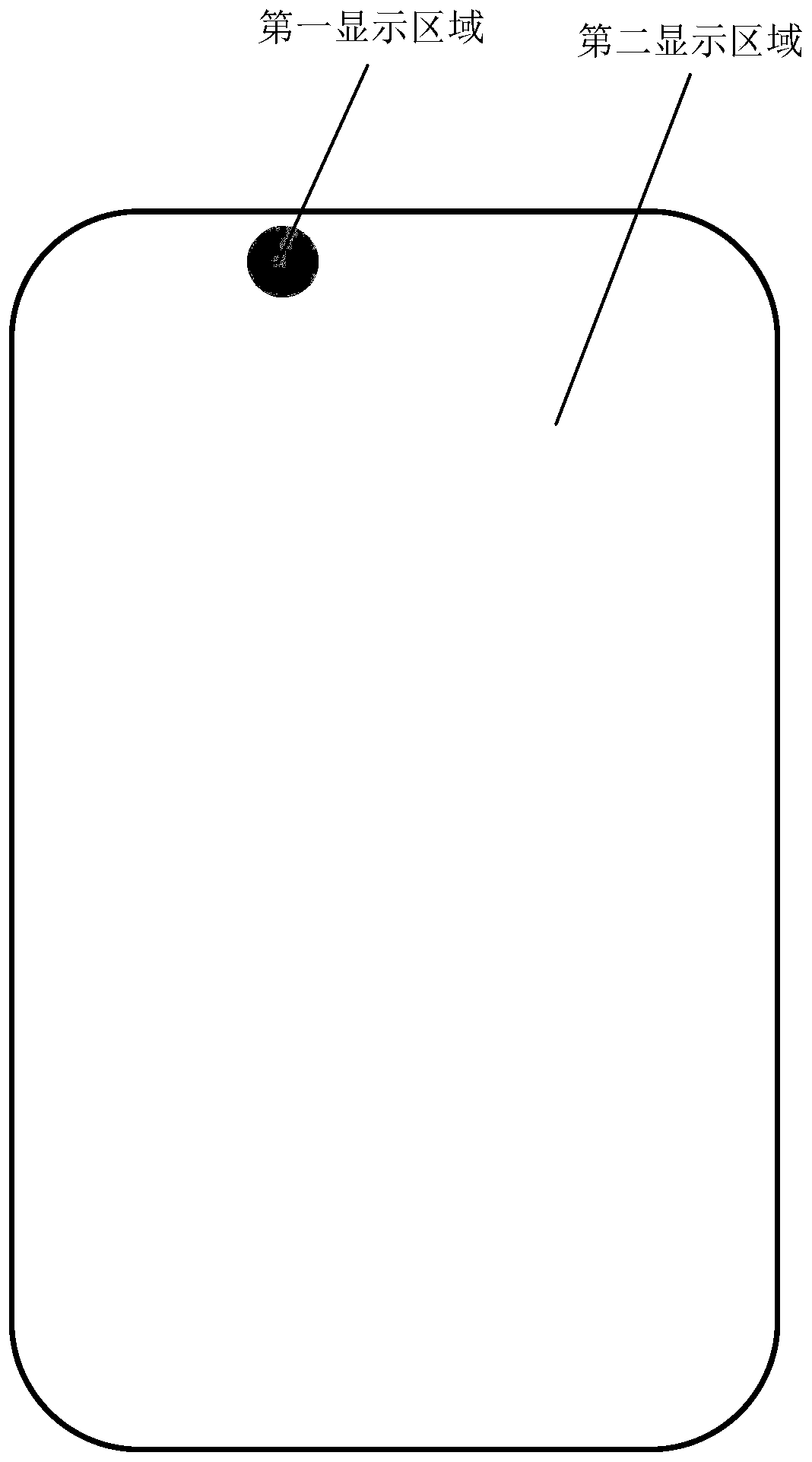
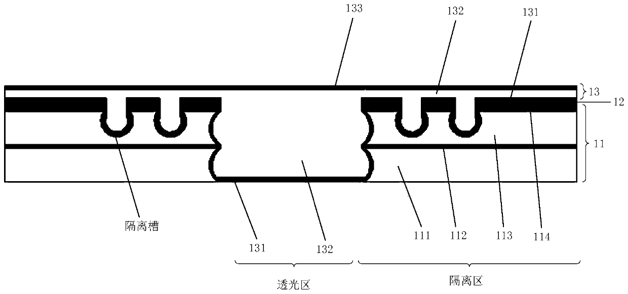
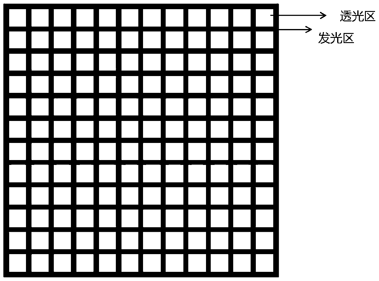
[0040] An embodiment of the present application provides a display substrate, referring to figure 1 , the display substrate includes a first display area and a second display area, the first display area includes a plurality of first pixel areas, the second display area includes a plurality of second pixel areas, and the density of the first pixel area is smaller than that of the second pixel area Density, see figure 2 Each first pixel area includes a light-transmitting area and an isolation area arranged around the light-transmitting area, wherein the display substrate in the isolation area includes a substrate 11, an organic light-emitting layer 12 (EL layer) arranged on one side of the substrate 11, and an organic light-emitti...


PUM


Abstract

The invention provides a preparation method of a display substrate, the display substrate and a display device. The display substrate comprises a first display region and a second display region, wherein the first display region comprises a plurality of first pixel regions, the second display area comprises a plurality of second pixel regions, the density of the first pixel regions is less than that of the second pixel regions, each first pixel region comprises a light-transmitting region and an isolation region arranged at the periphery of the light-transmitting region, the display substrateof the isolation region comprises a substrate, an organic light-emitting layer arranged at one side of the substrate and a packaging layer arranged at the side, which deviates from the substrate, of the organic light-emitting layer, the organic light-emitting layer in the isolation region is discontinuous, and the packaging layer covers the light-transmitting region. According to the technical scheme, transparent display is achieved by arranging the light-transmitting region in the first display region, the light transmittance of the first display region is improved, the optical device can bearranged in the first display region, and thus real full-screen display is achieved.

Description

technical field [0001] The invention relates to the field of display technology, in particular to a method for preparing a display substrate, a display substrate and a display device. Background technique [0002] In recent years, a full-screen display device has become one of the hot technologies in the field of display technology. However, although the screens of display devices that have been mass-produced in related technologies are called full screens, they are actually "notch screens". Integrate optical components such as front camera and infrared sensor. Therefore, it is necessary to punch holes or set notch areas on the screen to integrate optical components to realize the functions of optical components in the display device. Therefore, in the current related technologies, only "notch screens" can be realized, and it is impossible to realize full screen. Contents of the invention [0003] The invention provides a method for preparing a display substrate, a disp...

Claims


Application Information

Patent Timeline
Patent Type & Authority Applications(China)
IPC IPC(8): H01L51/56H01L51/50H01L51/52H01L27/32
CPCH10K59/00H10K50/84H10K50/11H10K71/00Y02E10/549
Inventor 孙阔田学伟
Owner BOE TECH GRP CO LTD
Why Eureka
Try Eureka