Display panel
A technology for display panels and display areas, applied in electrical components, electrical solid-state devices, circuits, etc., and can solve problems such as cracks, thin film transistor failure, and metal wire breakage.
- Summary
- Abstract
- Description
- Claims
- Application Information
AI Technical Summary
Problems solved by technology
Method used
Image

Examples
Embodiment Construction
[0028] In order to better understand the content of the present invention, the present invention will be further described through specific examples below, but the implementation and protection scope of the present invention are not limited thereto.
[0029] The following description of the embodiments refers to the accompanying drawings to illustrate specific embodiments in which the invention may be practiced. The directional terms mentioned in the present invention, such as "up", "down", "front", "back", "left", "right", "top", "bottom", etc., are only for reference to the attached drawings. direction. Therefore, the directional terms used are used to illustrate and understand the present invention, but not to limit the present invention.
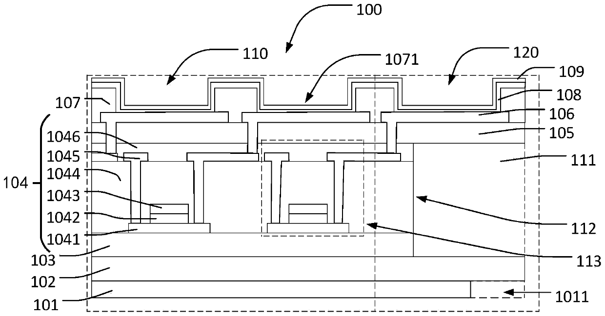
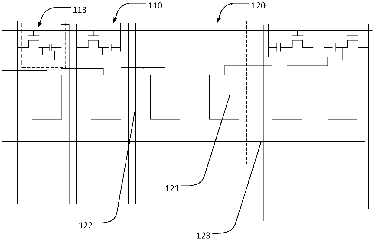
[0030] The present invention provides a display panel, comprising: a flexible substrate, a buffer layer, a thin film transistor layer, a planarization layer and a first electrode.
[0031] The flexible substrate has a main display area...
PUM
 Abstract
Description
Claims
Application Information
 - R&D Engineer
- R&D Manager
- IP Professional
- Industry Leading Data Capabilities
- Powerful AI technology
- Patent DNA Extraction
Browse by: Latest US Patents, China's latest patents, Technical Efficacy Thesaurus, Application Domain, Technology Topic.
© 2024 PatSnap. All rights reserved.Legal|Privacy policy|Modern Slavery Act Transparency Statement|Sitemap