Check patentability & draft patents in minutes with Patsnap Eureka AI!

Surface grating semiconductor laser and manufacturing method thereof

A technology of surface grating and manufacturing method, which is applied in the direction of semiconductor lasers, optical waveguide semiconductor structures, lasers, etc., and can solve the problems of high price, unfavorable mass production of devices, and long processing time

Active Publication Date: 2021-05-18
INST OF SEMICONDUCTORS - CHINESE ACAD OF SCI
View PDF18 Cites 2 Cited by
  • Summary
  • Abstract
  • Description
  • Claims
  • Application Information

AI Technical Summary

Problems solved by technology

Therefore, most surface grating lasers are produced by electron beam lithography, but this equipment is expensive and takes a long time to process, which is not conducive to mass production of devices

Method used


Image

  • Surface grating semiconductor laser and manufacturing method thereof
  • Surface grating semiconductor laser and manufacturing method thereof
  • Surface grating semiconductor laser and manufacturing method thereof

Examples


Embodiment Construction

[0018] In order to make the object, technical solution and advantages of the present invention clearer, the present invention will be further described in detail below in conjunction with specific embodiments and with reference to the accompanying drawings.

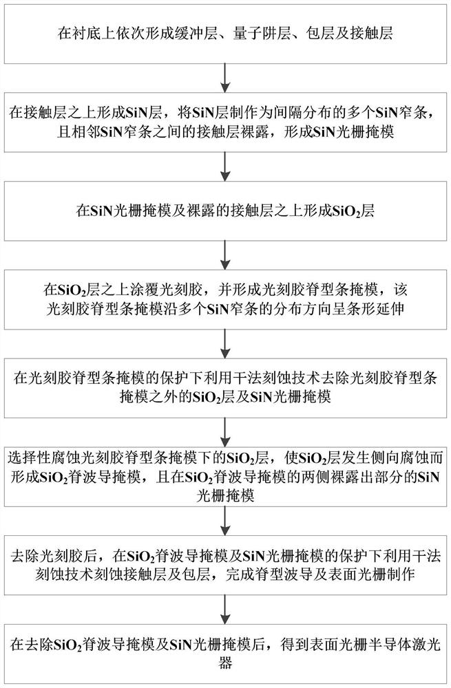
[0019] The invention discloses a surface grating semiconductor laser and a manufacturing method thereof. The surface gratings located on both sides of a ridge waveguide are fabricated by adopting a common photolithography process, which is beneficial to reducing the manufacturing cost of the device.

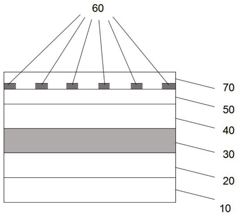
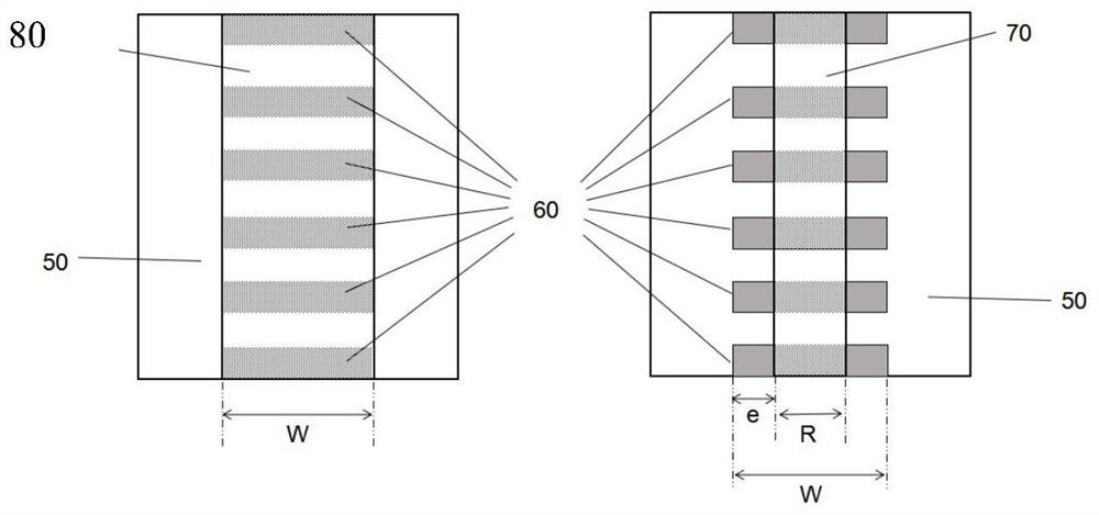
[0020] Specifically, as an exemplary embodiment of the present invention, a surface grating semiconductor laser and a manufacturing method thereof are provided. see figure 1 , taking the InP-based material system as an example, but not limited thereto, it can also be other material systems such as silicon-based material systems, etc. The method for manufacturing the surface semiconductor laser includes the following steps: ...


PUM


Abstract

A surface grating semiconductor laser and a manufacturing method thereof, comprising the following steps: sequentially growing a buffer layer, a quantum well layer, a cladding layer, and a contact layer on a substrate; depositing a SiN layer on the contact layer, and making a SiN grating mask; Deposition of SiO on SiN grating mask and exposed contact layer 2 layer; in SiO 2 Coating photoresist on the layer, and making a photoresist ridge strip mask; using dry etching technology to remove SiO outside the photoresist ridge strip mask 2 layer and SiN grating mask; using selective etching of SiO 2 layer, making SiO 2 The layer undergoes lateral corrosion to form SiO 2 Ridge waveguide mask; photoresist removed, on SiO 2 Under the protection of the ridge waveguide mask and the SiN grating mask, the contact layer and the cladding layer are etched by dry etching technology to complete the fabrication of the ridge waveguide and the surface grating. The surface gratings of the device located on both sides of the ridge waveguide of the present invention can be realized by ordinary photolithography technology, which is beneficial to reduce the manufacturing cost of the device.

Description

technical field [0001] The invention relates to the field of optoelectronic devices, in particular to a surface grating semiconductor laser and a manufacturing method thereof. Background technique [0002] Introducing a distributed feedback grating structure is an important means to obtain a single-mode semiconductor laser, which is called a distributed feedback (DFB) laser. Taking the InGaAsP / InP material system as an example, the conventional DFB laser grating is located between the InGaAsP quantum well and the InP cladding material. Two MOCVD epitaxial growths are required to complete the device fabrication, that is, the quantum well material is obtained in the first growth, and the InP cladding material is grown in the second epitaxy after the grating is fabricated. In order to simplify the device fabrication process, DFB lasers with surface grating structures have been developed. The quantum well and cladding material of this device can be grown in a single epitaxy, a...

Claims


Application Information

Patent Timeline
Patent Type & Authority Patents(China)
IPC IPC(8): H01S5/125H01S5/22
CPCH01S5/1231H01S5/125H01S5/22
Inventor 梁松
Owner INST OF SEMICONDUCTORS - CHINESE ACAD OF SCI
Features
  • R&D
  • Intellectual Property
  • Life Sciences
  • Materials
  • Tech Scout
  • Unparalleled Data Quality
  • Higher Quality Content
  • 60% Fewer Hallucinations
Learn More