Load detection circuit, SOC system, and configuration method of load detection circuit
A technology for detecting circuits and configuration methods, applied in the direction of electronic circuit testing, measuring electricity, measuring devices, etc., can solve the problem that there is no good solution for load detection.
- Summary
- Abstract
- Description
- Claims
- Application Information
AI Technical Summary
Problems solved by technology
Method used
Image

Examples
Embodiment approach 1
[0081] [Multi-power domain SOC system]
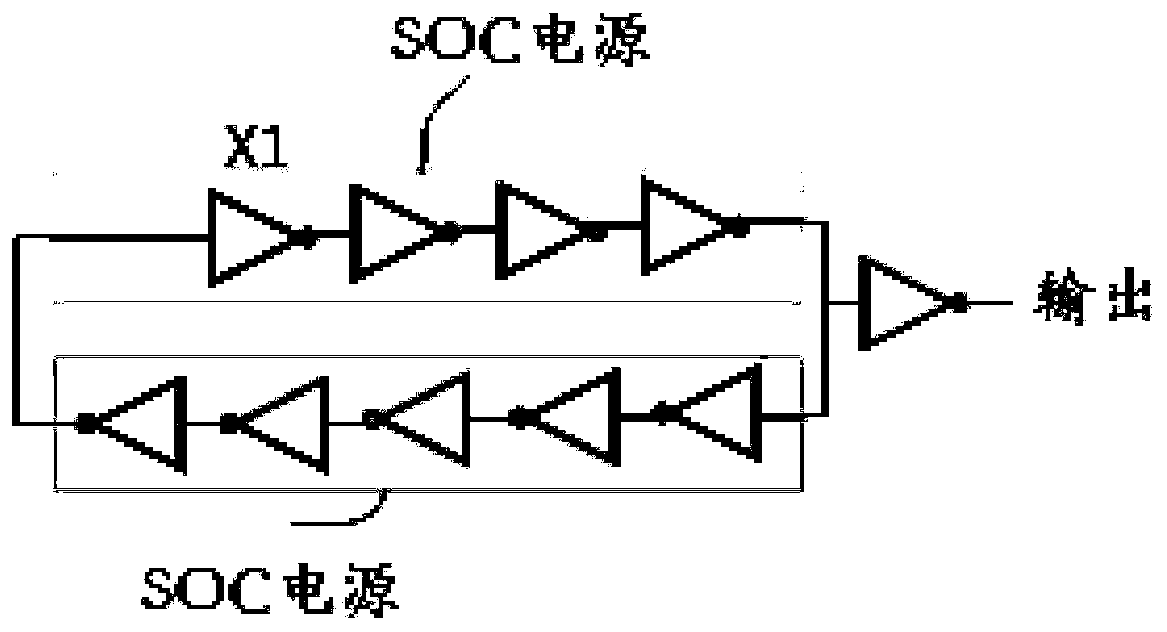
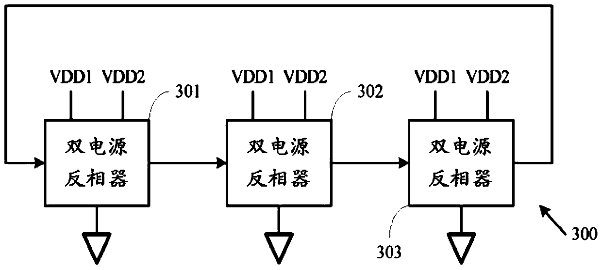
[0082] Figure 5 A block diagram of a load detection module in the SOC system according to Embodiment 1 of the present invention is shown. exist Figure 5 In the figure, it is shown that the SOC system includes two power domains, the first power domain and the second power domain, which are arranged in series, supplying power supply voltages VDD1 and VDD2 to different modules respectively, and multiple delays are respectively configured for each power domain Unit Z1, these delay units Z1 are connected in series with each other to form a ring oscillator.
[0083] In the present invention, the delay units Z1 arranged in the respective power domains have basically the same circuit structure.
[0084] It should be noted that, in order to simplify the description, it is illustrated that the SOC system includes 2 power domains, but the SOC system may include more than 3 power domains. In addition, in the embodiment, the SOC system is used...
Embodiment 1
[0093] In the simulation, in the above step s1, the critical path is fitted to obtain the delay time of each power domain, and the set voltage of each power domain is the actual working voltage. Assuming that the voltage VDD1 of the first power domain is 1v, the delay time of the first power domain is 1 nanosecond (ns), the voltage VDD2 of the second power domain is 1.2v, and the delay time of the second power domain is 1.5 nanoseconds ( ns).
[0094] In the above step S2, the delay of the configurable delay unit under VDD1 and VDD2 is fitted, if the delay of the delay unit under VDD1 is 10 picoseconds (ps), and the delay under VDD2 is 8 picoseconds (ps), then In the entire ring oscillator, the number of delay units in the first power domain is 1ns / 10ps=100, the number of delay units in the second power domain is 1.5ns / 8ps=187.5, and the nearest integer is 188 . Accordingly, in the ring oscillator, the stage ratio of the delay cells arranged in the first power supply domain ...
Embodiment 2
[0100] In the simulation, in the above step s1, the critical path is fitted to obtain the delay time of each power domain, and the set voltage of each power domain is the actual working voltage. Assuming that the voltage VDD1 of the first power domain is 1v, the delay time of the first power domain is 1 nanosecond (ns), the voltage VDD2 of the second power domain is 1.2v, and the delay time of the second power domain is 1.6 nanoseconds ( ns).
[0101] In the above step S2, fitting the delay of the configurable power delay unit under VDD1 and VDD2, if the delay of the delay unit under VDD1 is 10 picoseconds (ps), and the delay under VDD2 is 8 picoseconds (ps), Then, in the whole ring oscillator, the number of delay units selected for the first power domain is 1 ns / 10 ps=100, and the number of delay units selected for the second power domain is 1.6 ns / 8 ps=200. Accordingly, in the ring oscillator, the stage ratio of the delay cells arranged in the first power supply domain and ...
PUM
 Abstract
Description
Claims
Application Information
 - R&D
- Intellectual Property
- Life Sciences
- Materials
- Tech Scout
- Unparalleled Data Quality
- Higher Quality Content
- 60% Fewer Hallucinations
Browse by: Latest US Patents, China's latest patents, Technical Efficacy Thesaurus, Application Domain, Technology Topic, Popular Technical Reports.
© 2025 PatSnap. All rights reserved.Legal|Privacy policy|Modern Slavery Act Transparency Statement|Sitemap|About US| Contact US: help@patsnap.com