Method for layout wiring of transistors in to-be-tested array one by one

A transistor and wiring technology, which is applied in the field of layout and wiring of transistors in the array to be tested one by one, can solve the problems of small feature size, increased complexity, and inability to meet the needs of integrated circuit design, and can ensure the quality of wiring and save time. Effect

Pending Publication Date: 2020-07-24
SEMITRONIX
View PDF6 Cites 0 Cited by
  • Summary
  • Abstract
  • Description
  • Claims
  • Application Information

AI Technical Summary

Problems solved by technology

[0002] With the rapid development of integrated circuit technology, integrated circuits have entered the era of ultra-deep submicron, which makes the feature size of electronic devices smaller and smaller, the scale of chips is larger and larger, and more and more components can be integrated in a single On the chip, the complexity has risen sharply, and for the wiring method in the layout, the manual design wiring method has long been unable to meet the needs of integrated circuit design, and the computer automatic wiring has occupied an increasing proportion in the layout design and wiring.

Method used


Image

  • Method for layout wiring of transistors in to-be-tested array one by one
  • Method for layout wiring of transistors in to-be-tested array one by one
  • Method for layout wiring of transistors in to-be-tested array one by one

Examples


Embodiment Construction

[0059] Below in conjunction with accompanying drawing and specific embodiment the present invention is described in further detail:

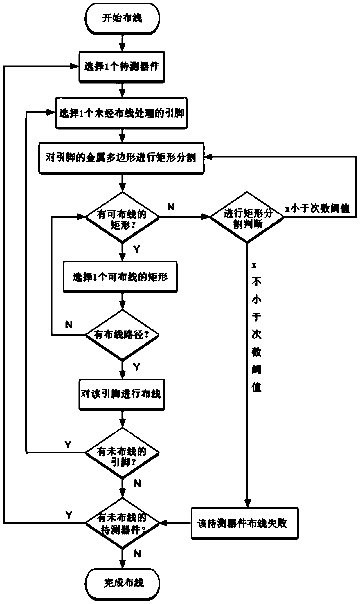
[0060] A method for performing layout and wiring of transistors in an array to be tested one by one, including a preprocessing process and a wiring process; the method can ensure the quality of wiring and save time while processing and wiring the devices to be tested one by one. The following is a detailed introduction.

[0061] The preprocessing process specifically includes the following steps:

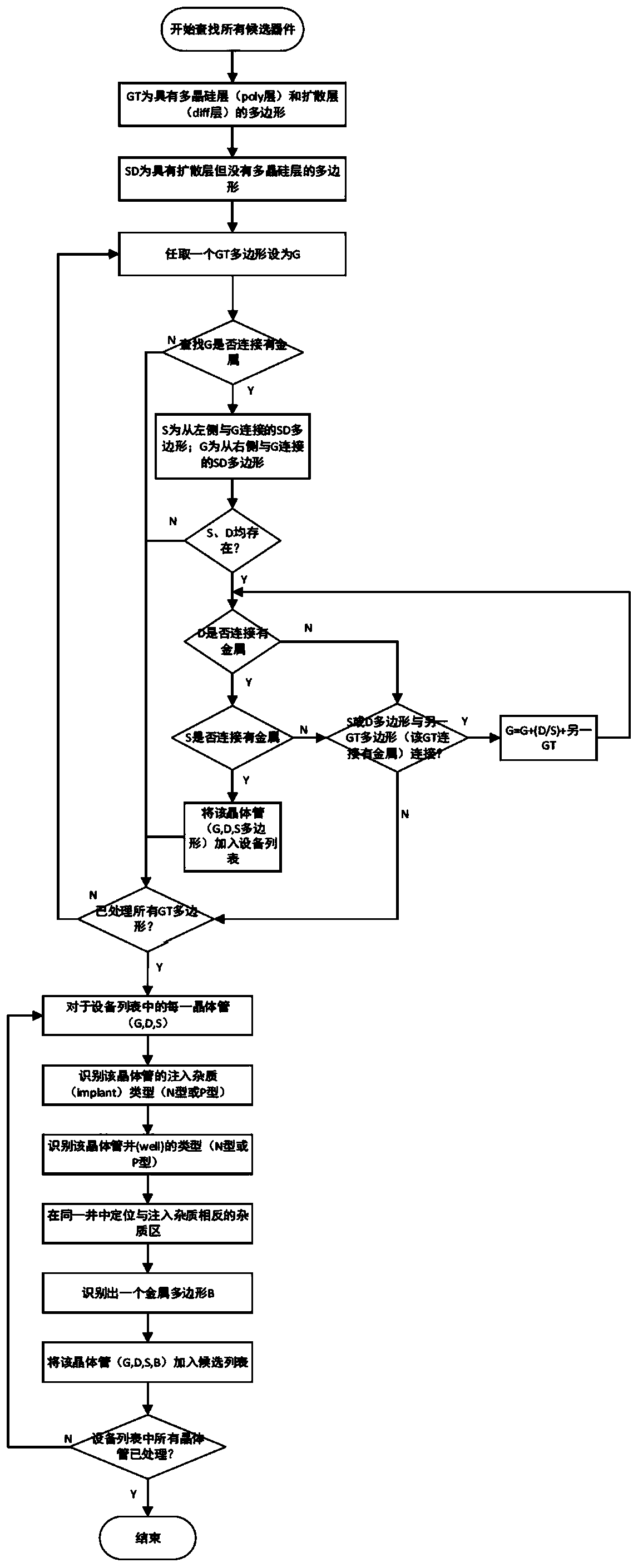
[0062] Step (1): If the locations of all candidate devices (DUTs) are known, directly import the location information; if the locations of candidate devices are not known, search to obtain the locations of all candidate devices. After obtaining the positions of all candidate devices, determine the device under test corresponding to each metal frame (frame) from the candidate devices. Candidate devices in the center of the frame; each metal frame cor...


PUM


Abstract

The invention relates to a method for layout wiring of transistors in a to-be-tested array one by one. The method comprises a preprocessing process and a wiring process. The method includes: determining that the candidate device corresponds to the metal frame through a preprocessing process and determining the position of the candidate device; and wiring each pin of the to-be-tested device throughthe wiring process. According to the invention, the wiring quality is ensured and the time is saved while the to-be-tested devices are processed and wired one by one.

Description

technical field [0001] The invention relates to the technical field of integrated circuits, in particular to a method for layout layout and wiring of transistors in an array to be tested one by one. Background technique [0002] With the rapid development of integrated circuit technology, integrated circuits have entered the era of ultra-deep submicron, which makes the feature size of electronic devices smaller and smaller, the scale of chips is larger and larger, and more and more components can be integrated in a single On the chip, the complexity has risen sharply, and for the wiring method in the layout, the manual design wiring method has long been unable to meet the needs of integrated circuit design, and computer automatic wiring has occupied an increasing proportion of layout design and wiring. [0003] For the test chip, the transistors integrated on it can be different, and these transistors form the array to be tested, which means that each device to be tested mus...

Claims


Application Information

Patent Timeline
IPC IPC(8): G06F30/392
Inventor 蓝帆
Owner SEMITRONIX
Why Eureka
Try Eureka