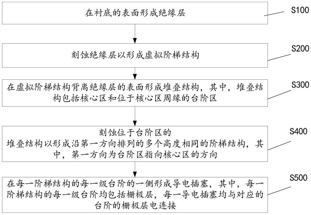
Eureka AIR delivers breakthrough ideas for toughest innovation challenges, trusted by R&D personnel around the world.

Three-dimensional memory and its preparation method

A memory and three-dimensional technology, applied in the direction of semiconductor devices, electrical solid devices, electrical components, etc., can solve the problems of increased process and material costs and difficult contact parts, and achieve the effect of reducing process and material costs and balancing depth differences

Active Publication Date: 2021-09-07
YANGTZE MEMORY TECH CO LTD
View PDF0 Cites 0 Cited by
  • Summary
  • Abstract
  • Description
  • Claims
  • Application Information

AI Technical Summary

Problems solved by technology

[0003] In view of this, the present application provides a three-dimensional memory and its preparation method to solve the problem of increasing the difficulty of etching all the contacts in a single step as the number of stacked layers and the stacking height continue to increase in the prior art. , easily lead to the increase of process and material cost

Method used


Image

  • Three-dimensional memory and its preparation method
  • Three-dimensional memory and its preparation method
  • Three-dimensional memory and its preparation method

Examples


Embodiment Construction

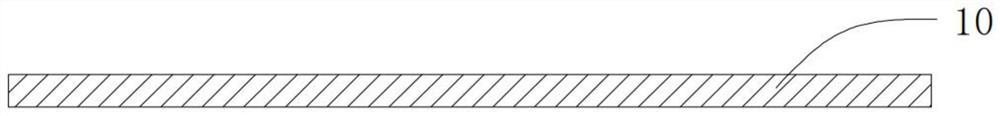
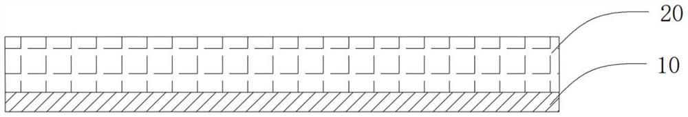
[0041] Specific embodiments of the present invention will be described in more detail below with reference to the accompanying drawings. Although exemplary embodiments of the invention are shown in the drawings, it should be understood that the invention may be practiced in other ways than those described herein, and therefore, the invention is not limited by the following embodiments.

[0042] In a three-dimensional memory such as 3D NAND flash memory, the memory array may include a core area (Core) and a stair case area (Staircase structure, SS). The step region is used to lead out contacts for the gate layer in each layer of the memory array. These gate layers are used as word lines of the memory array to perform operations such as programming, erasing, and reading.

[0043] In the manufacturing process of the three-dimensional memory, contact holes are formed by etching on the step structures of all levels in the step region, and then the contact holes are filled, so as t...


PUM


Abstract

The present application provides a three-dimensional memory and its preparation method, including: forming an insulating layer on the surface of the substrate; etching the insulating layer to form a virtual ladder structure; forming a stack structure on the surface of the virtual ladder structure away from the insulating layer, wherein the stack structure Including a core area and a stepped area located around the core area; etching the stacked structure located in the stepped area to form a plurality of stepped structures of the same height arranged along a first direction, wherein the first direction is a direction in which the stepped area points to the core area; Conductive plugs are formed on one side of each step of each stepped structure, wherein each step of each stepped structure includes a gate layer, and each conductive plug is electrically connected to the gate layer of the corresponding step. connect. The present application solves the problem in the prior art that as the number of stacked layers and stacking height continue to increase, it becomes more and more difficult to etch all the contact parts at a single time, which easily leads to an increase in process and material costs.

Description

technical field [0001] The invention relates to the technical field of semiconductors, in particular to a three-dimensional memory and a preparation method thereof. Background technique [0002] In the three-dimensional memory manufacturing process, in order to ensure that the contact portion can be smoothly connected to the gate in each memory array, it is necessary to form a three-dimensional (3D) ladder structure. With the rapid development of three-dimensional memory technology, the number of stacked layers of the memory array on the substrate is increasing, so the number of steps on the ladder structure is also increasing, which in turn leads to the closer to the step of the substrate, the etching forms the contact part connecting it The more difficult it is to etch, as the number of stacked layers and the stacking height continue to increase, the difficulty of etching all the contact parts at a single time will also become more and more difficult, which will easily lea...

Claims


Application Information

Patent Timeline
Patent Type & Authority Patents(China)
IPC IPC(8): H01L27/11524H01L27/11556H01L27/1157H01L27/11582
CPCH10B41/35H10B41/27H10B43/35H10B43/27
Inventor 孙中旺赵祥辉胡军张中周文犀
Owner YANGTZE MEMORY TECH CO LTD
Why Eureka
Eureka Blog
Learn More