Flexible smart piezoelectric sensor based on pentacene organic field-effect transistor coupled with PVDF nanopillars
An intelligent piezoelectric and pentacene technology, which can be used in the manufacture of semiconductor devices, electro-solid devices, and semiconductor/solid-state devices, and can solve the problems of low piezoelectric strain constant and limited charge.
- Summary
- Abstract
- Description
- Claims
- Application Information
AI Technical Summary
Problems solved by technology
Method used
Image
Examples
Embodiment 1
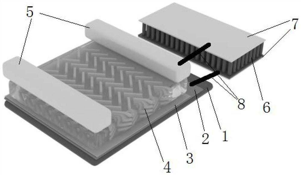
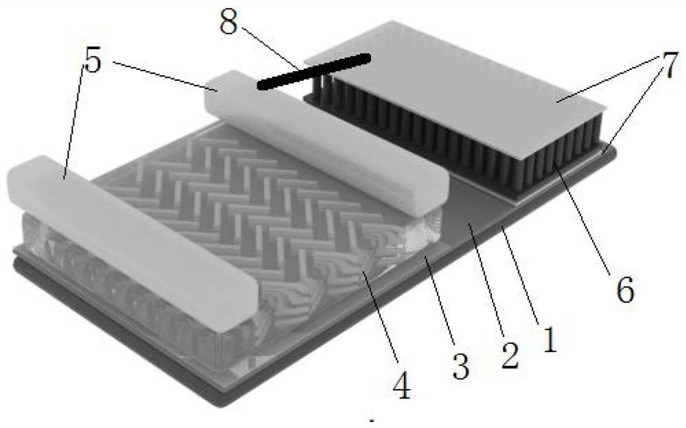
[0048] (1) Ultrapure water, acetone solution, and isopropanol were used to ultrasonically clean the experimental-grade PET film substrate for 10 minutes, and then the PET substrate was cleaned with an oxygen plasma cleaner for 10 minutes and dried in a nitrogen environment; the clean PET substrate was placed on the into the metal vacuum coater to the s -1 Deposit Al with a thickness of about 100nm as the bottom gate electrode; Next, configure a PMMA solution of 7mg / ml and use a spin coater to form a PMMA film of about 400nm on the aluminum electrode at a rate of 4000rpm as the dielectric layer of the device, and in a vacuum Treat in a drying oven at 60°C for 2 hours; then use an organic vacuum coater to the s -1 Deposit 40nm-thick organic small molecule material pentacene at a rate of 40nm to form an active layer to transport charges; then use a transmission electron microscope copper mesh (200um in length, 40um in width, and 20um in channel width) as a mask on the pentace...
Embodiment 2
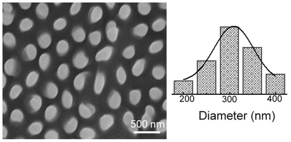
[0052] (1) Ultrapure water, acetone solution, and isopropanol were used to ultrasonically clean the experimental-grade PET film substrate for 10 minutes, and then the PET substrate was cleaned with an oxygen plasma cleaner for 10 minutes and dried in a nitrogen environment; the clean PET substrate was placed on the into the metal vacuum coater to the s -1 Deposit Al with a thickness of about 100nm as the bottom gate electrode; Next, configure a PMMA solution of 7mg / ml and use a spin coater to form a PMMA film of about 400nm on the aluminum electrode at a rate of 4000rpm as the dielectric layer of the device, and in a vacuum Treat in a drying oven at 60°C for 2 hours; then use an organic vacuum coater to the s -1 Deposit 40nm-thick organic small molecule material pentacene at a rate of 40nm to form an active layer to transport charges; then use a transmission electron microscope copper mesh (200um in length, 40um in width, and 20um in channel width) as a mask on the pentace...
PUM
| Property | Measurement | Unit |
|---|---|---|
| thickness | aaaaa | aaaaa |
| thickness | aaaaa | aaaaa |
| Sensitivity | aaaaa | aaaaa |
Abstract
Description
Claims
Application Information


