Flexible intelligent piezoelectric sensor based on coupling of pentacene organic field effect transistor and PVDF nanorod
A smart piezoelectric and pentacene technology, which is applied in the manufacture of electric solid-state devices, semiconductor devices, semiconductor/solid-state devices, etc., can solve the problems of low piezoelectric strain constant and limited charge
- Summary
- Abstract
- Description
- Claims
- Application Information
AI Technical Summary
Problems solved by technology
Method used
Image
Examples
Embodiment 1
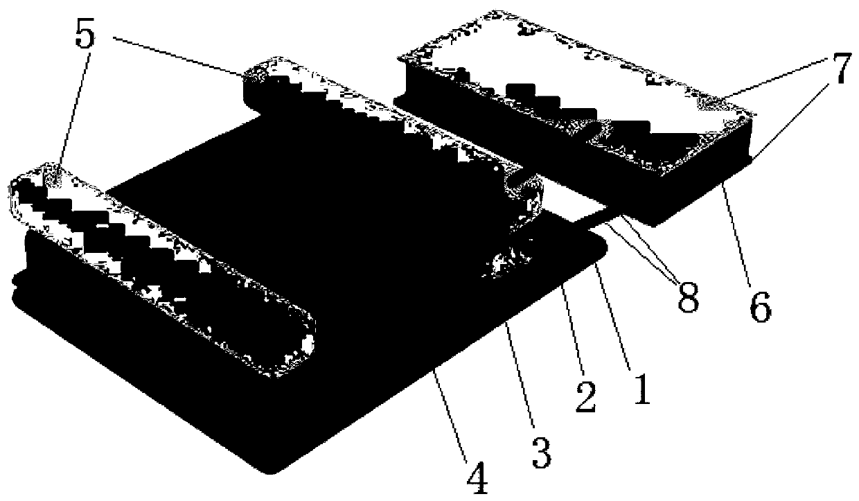
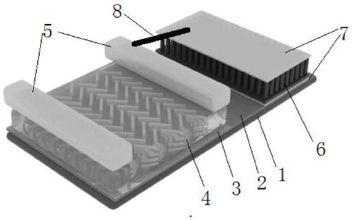
[0048] (1) The experimental PET film substrate was ultrasonically cleaned with ultrapure water, acetone solution and isopropanol for 10 minutes, and then the PET substrate was cleaned with an oxygen plasma cleaner for 10 minutes and dried in a nitrogen environment; the clean PET substrate was placed Into the metal vacuum coating instrument to s -1 Deposit about 100nm thick Al as the bottom gate electrode at a rate of about 100nm; then configure 7mg / ml PMMA solution and use a spin coater to form a 400nm PMMA film on the aluminum electrode at a rate of 4000rpm as the dielectric layer of the device. Treat for 2h at 60℃ in a drying oven; then use an organic vacuum coating instrument to s -1 Depositing a 40nm thick organic small molecule material pentacene to form an active layer to transport charges at a rate of 5%; then using a transmission electron microscope copper mesh (length 200um, width 40um, channel width 20um) as a mask on the pentacene film A metal vacuum coater was used...
Embodiment 2
[0052] (1) The experimental PET film substrate was ultrasonically cleaned with ultrapure water, acetone solution and isopropanol for 10 minutes, and then the PET substrate was cleaned with an oxygen plasma cleaner for 10 minutes and dried in a nitrogen environment; the clean PET substrate was placed Into the metal vacuum coating instrument to s -1 Deposit about 100nm thick Al as the bottom gate electrode at a rate of about 100nm; then configure 7mg / ml PMMA solution and use a spin coater to form a 400nm PMMA film on the aluminum electrode at a rate of 4000rpm as the dielectric layer of the device. Treat for 2h at 60℃ in a drying oven; then use an organic vacuum coating instrument to s -1 Depositing a 40nm thick organic small molecule material pentacene to form an active layer to transport charges at a rate of 5%; then using a transmission electron microscope copper mesh (length 200um, width 40um, channel width 20um) as a mask on the pentacene film A metal vacuum coater was used...
PUM
| Property | Measurement | Unit |
|---|---|---|
| thickness | aaaaa | aaaaa |
| concentration | aaaaa | aaaaa |
| length | aaaaa | aaaaa |
Abstract
Description
Claims
Application Information


