Memory and forming method thereof

A memory and graphics technology, which is applied in the manufacture of electrical solid-state devices, semiconductor devices, and semiconductor/solid-state devices, etc., and can solve the problems of low etching rate of conductive material layers, large lateral undercutting, and the influence of node contact structure morphology.

Pending Publication Date: 2020-09-08
FUJIAN JINHUA INTEGRATED CIRCUIT CO LTD
View PDF0 Cites 3 Cited by
  • Summary
  • Abstract
  • Description
  • Claims
  • Application Information

AI Technical Summary

Problems solved by technology

[0007] However, it should be noted that, in the above-mentioned preparation method, on the one hand, the hardness of the conductive material used to form the node contact structure is usually relatively high, so that the etching rate of the conductive material layer is relatively low during the etching process. low, and will also produce a large lateral undercutting phenomenon, which will affect the morphology

Method used


Image

  • Memory and forming method thereof
  • Memory and forming method thereof
  • Memory and forming method thereof

Examples


Embodiment Construction

[0065] The memory and its forming method proposed by the present invention will be further described in detail below with reference to the drawings and specific embodiments. The advantages and features of the present invention will become clearer from the following description. It should be noted that all the drawings are in a very simplified form and use imprecise scales, and are only used to facilitate and clearly assist the purpose of illustrating the embodiments of the present invention.

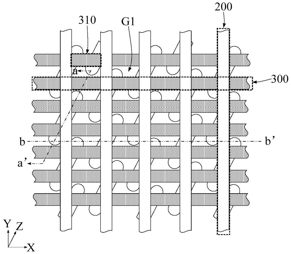
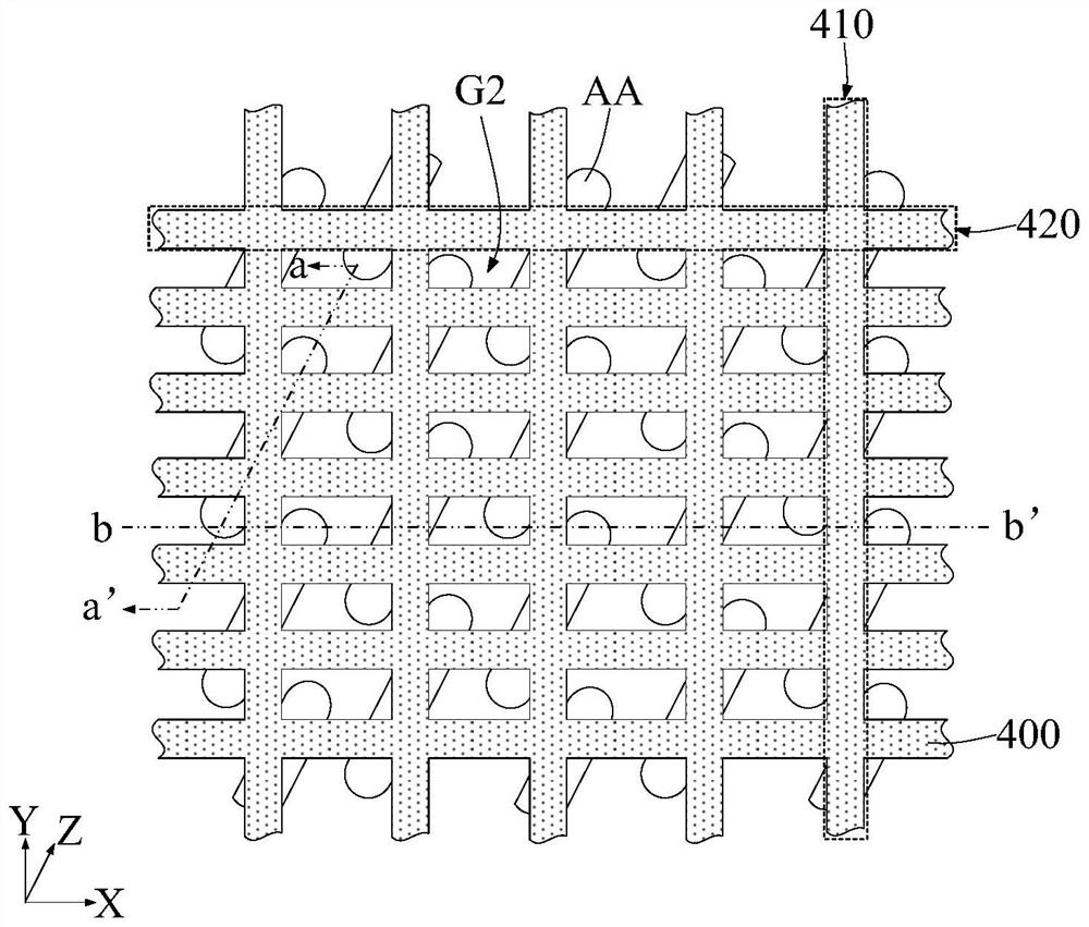
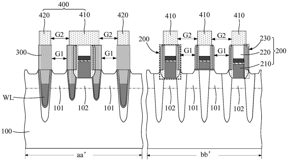
[0066] Figure 1a is a memory in an embodiment of the present invention, which illustrates a top view of a first lattice array of node contacts, Figure 1b is a memory in an embodiment of the present invention, which illustrates a top view of a second gridded array of node contacts, figure 2 is a schematic cross-sectional view of a memory device in an embodiment of the present invention showing a node contact window, image 3 It is a schematic cross-sectional view of a memory device i...


PUM


Abstract

The invention provides a memory and a forming method thereof. A bit line and an insulating line are used for defining a first grid array, after the bit lines and the insulating lines are formed, the isolation layer is used for further defining the second lattice array corresponding to the first lattice array, so that the first lattice array and the second lattice array can be combined to define the node contact window, and then the node contact structure can be filled in the node contact window in a self-aligned mode. Therefore, according to the memory and the forming method thereof, when a node contact structure is prepared, a graphical process does not need to be executed on a conductive material used for forming the node contact structure, thus, the etching process in the patterning process of the conductive material with high hardness can be omitted, the pattern precision of the formed node contact structure can be improved, polymers can be prevented from being generated, and the polymers are prevented from being attached to the node contact structure.

Description

technical field [0001] The invention relates to the technical field of semiconductors, in particular to a memory and a forming method thereof. Background technique [0002] Memory, such as dynamic random access memory (Dynamic Random Access Memory, DRAM), which generally includes a storage capacitor and a storage transistor electrically connected to the storage capacitor, the storage capacitor is used to store charges representing stored information, and the storage transistor The storage capacitor can be electrically connected through a node contact structure. [0003] Wherein, the preparation method of the node contact structure generally includes: [0004] Firstly, depositing a layer of conductive material on the substrate, and forming a mask layer on the layer of conductive material, so as to use the mask layer to define the pattern of the node contact structure; [0005] Next, etching the conductive material layer using the mask layer as a mask, so as to copy the patt...

Claims


Application Information

Patent Timeline
IPC IPC(8): H01L27/108H01L21/8242
CPCH10B12/315H10B12/0335
Inventor 赖惠先林昭维朱家仪张钦福
Owner FUJIAN JINHUA INTEGRATED CIRCUIT CO LTD
Why Eureka
Try Eureka