Metal heat-conducting substrate and manufacturing method thereof

A heat-conducting substrate and manufacturing method technology, applied in the direction of circuit substrate materials, semiconductor/solid-state device manufacturing, semiconductor devices, etc., can solve the problems of poor reliability, complex process, poor high and low temperature stability of epoxy resin, etc., to avoid high temperature sintering, The effect of saving metal materials and expanding the variety of materials

Inactive Publication Date: 2012-12-26
SHENZHEN UNIV
View PDF0 Cites 1 Cited by
  • Summary
  • Abstract
  • Description
  • Claims
  • Application Information

AI Technical Summary

Problems solved by technology

[0003] At present, the more common ceramic substrates on the market are mostly LTCC (Low Temperature Co-fired Ceramic LTCC) or ceramic heat dissipation substrates made of thick film technology. The calibration bottleneck of hand-screen printing technology for this type of products makes Its alignment accuracy cannot be matched with further soldering, such as eutectic or flip-chip packaging
[0004] It is more common in the prior art that epoxy resin is used for the insulating medium layer, and a copper circuit layer is adhered to it; the main problems are: 1. Poor thermal conductivity of epoxy resin; 2. Poor high and low temperature stability of epoxy resin; 3. The high temperature cracking of epoxy resin causes poor reliability, and the connection strength between epoxy resin and copper circuit layer and substrate is not high; 4. The process of manufacturing circuits is complex, polluting, not environmentally friendly, and unnecessary copper circuit layers need to be corroded, waste of copper resources

Method used


Image

  • Metal heat-conducting substrate and manufacturing method thereof
  • Metal heat-conducting substrate and manufacturing method thereof
  • Metal heat-conducting substrate and manufacturing method thereof

Examples


Embodiment Construction

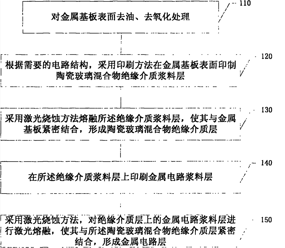
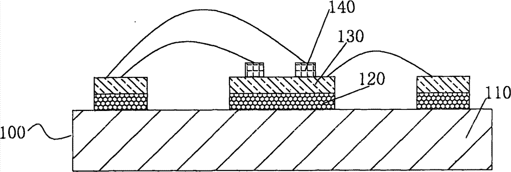
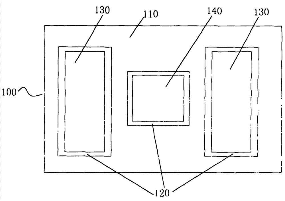
[0040] A metal thermally conductive substrate and its manufacturing method provided by the present invention use printing and laser ablation melting methods to manufacture metal-based ceramic glass mixture insulating film insulating film thermally conductive PCB substrates on metal, which are used for power LD, LED and power electronic devices , sensor packaging, circuit connection, and provide good heat dissipation channels. In order to make the purpose, technical solutions and advantages of the present invention clearer and clearer, the present invention will be further described in detail below with reference to the accompanying drawings and examples. It should be understood that the specific embodiments described here are only used to explain the present invention, not to limit the present invention.

[0041] A method for manufacturing a metal thermally conductive substrate of the present invention, such as figure 1 shown, including the following steps:

[0042] Step 110,...


PUM


Abstract

The invention relates to the technical field of electronic packaging and discloses a metal heat-conducting substrate and a manufacturing method thereof. An insulating medium slurry layer is printed on a metal substrate and molten by a laser ablation method to form an insulating medium layer, and a metal circuit slurry layer is printed on the insulating medium layer and molten by the laser ablation method to form a metal circuit layer, so that a well-insulated radiating passage is provided. The laser melting method has the advantages of achieving extremely high pattern accuracy, contributing to product miniaturization and precision, simplifying the technology of a manufacturing process, preventing pollution, saving materials, lowering cost and achieving good radiating effect.

Description

technical field [0001] The invention relates to the technical field of electronic packaging, in particular to a metal thermally conductive substrate and a manufacturing method thereof. Background technique [0002] Since the rise of the junction temperature during LED operation will reduce the probability of luminous recombination, the lifespan and output luminous flux will also decrease with the increase of temperature. If the heat generated by the PN junction can be dissipated as soon as possible, it will not only improve the luminous efficiency of the product, but also improve the reliability and life of the product. LED chips also have strict requirements on the matching of the linear expansion coefficient of the substrate material. [0003] At present, the more common ceramic substrates on the market are mostly LTCC (Low Temperature Co-fired Ceramic LTCC) or ceramic heat dissipation substrates made of thick film technology. The calibration bottleneck of hand-screen prin...

Claims


Application Information

Patent Timeline
Patent Type & Authority Patents(China)
IPC IPC(8): H01L21/48H01L23/498H01L23/34H05K1/05
CPCH01L2224/48091H01L2224/48137H01L2224/73265H01L2924/00014
Inventor 柴广跃刘文王少华黄长统雷云飞刘沛徐光辉
Owner SHENZHEN UNIV
Why Eureka
Try Eureka