Mask layout correction method and mask layout

A mask and layout technology, which is applied in the fields of electrical components, semiconductor/solid-state device manufacturing, circuits, etc., can solve the problems of poor performance of semiconductor structures, and achieve the effects of improved performance, good shape, and high graphics accuracy

Active Publication Date: 2021-10-19
SEMICON MFG INT (SHANGHAI) CORP +1
View PDF8 Cites 0 Cited by
  • Summary
  • Abstract
  • Description
  • Claims
  • Application Information

AI Technical Summary

Problems solved by technology

[0004] However, the performance of existing semiconductor structures is still poor

Method used


Image

  • Mask layout correction method and mask layout
  • Mask layout correction method and mask layout
  • Mask layout correction method and mask layout

Examples


Embodiment Construction

[0049] As mentioned in the background, the performance of existing semiconductor structures is still poor. Now analyze and illustrate in conjunction with specific embodiment.

[0050] It should be noted that the "surface" in this specification is used to describe the relative positional relationship in space, and is not limited to direct contact.

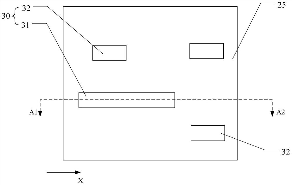
[0051] Figure 1 to Figure 11 It is a structural schematic diagram of each step in the formation process of a semiconductor structure.

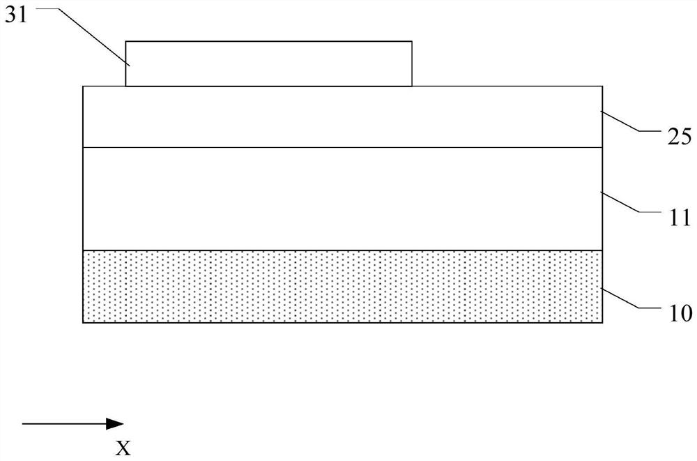
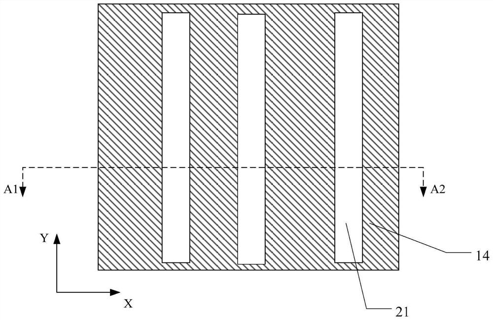
[0052] Please refer to Figure 1 to Figure 2 , figure 1 is a schematic top view of a semiconductor structure, figure 2 It is a schematic diagram of a cross-sectional structure along the A1-A2 direction in FIG. A cutting layer 30 is formed on the surface of the film material layer 25, and the cutting layer 30 includes a plurality of first strip structures 31 and second strip structures 32 extending along the first direction X. In the first direction X, the first The length of the strip struct...


PUM


Abstract

The invention discloses a mask layout correction method and a mask layout. The method comprises the steps that a first mask layout which comprises a plurality of first patterns extending along a first direction is formed; second mask layout information is obtained, the second mask layout information comprises a second mask layout, the second mask layout comprises a plurality of second patterns extending in the second direction, and after the first mask layout and the second mask layout are overlapped, the second patterns stretch across one or more first patterns, the second direction is perpendicular to the first direction; and the plurality of first patterns are compensated and corrected according to the layout information of the second mask. Therefore, the performance of the semiconductor structure is improved.

Description

technical field [0001] The invention relates to the technical field of semiconductors, in particular to a mask layout correction method and the mask layout. Background technique [0002] With the continuous improvement of semiconductor integrated circuit manufacturing technology, the continuous improvement of performance is also accompanied by the process of miniaturization and miniaturization of devices. More and more advanced manufacturing processes require as many devices as possible to be implemented in as small an area as possible. [0003] In very large-scale integrated circuits, the use of metal interconnection layers is one of the methods to realize the electrical interconnection between devices. Usually, a cutting layer (Metal-cut layer) is used to insulate adjacent metal interconnection layers, so that the distance between the ends of adjacent metal interconnection layers needs to be smaller than the exposure limit size of the exposure process to increase The den...

Claims


Application Information

Patent Timeline
Patent Type & Authority Applications(China)
IPC IPC(8): H01L21/033H01L21/66
CPCH01L22/24H01L21/0337H01L21/0338H01L22/30
Inventor 郑二虎张冬平洪中山
Owner SEMICON MFG INT (SHANGHAI) CORP
Why Eureka
Try Eureka