Three-dimensional radio frequency module manufacturing method based on multi-layer heat dissipation structure

A technology of radio frequency module and heat dissipation structure, which is applied in semiconductor/solid-state device manufacturing, electrical components, electric solid-state devices, etc. It can solve the problems of reduced heat dissipation capacity, inconsistent heat dissipation capacity of chip surface, and affecting chip reliability, etc., to achieve heat dissipation capacity consistent effect

Inactive Publication Date: 2020-09-11
浙江集迈科微电子有限公司
View PDF11 Cites 0 Cited by
  • Summary
  • Abstract
  • Description
  • Claims
  • Application Information

AI Technical Summary

Problems solved by technology

[0004] However, the embedding process of the silicon interposer needs to use a relatively harsh heat dissipation structure. For some radio frequency chips, if the area required for heat dissipation is large, there will be cooling liquid entering the microchannel at one end, followed by the heat dissipation on the chip. The distance of the bottom is getting bigger and bigger, and the temperature is getting higher and higher, which leads to the greatly reduced heat dissipation when it is left at the other end of the chip, which in turn causes inconsistent heat dissipation on the surface of the chip, which greatly affects the reliability of the chip when it is working.

Method used


Image

  • Three-dimensional radio frequency module manufacturing method based on multi-layer heat dissipation structure
  • Three-dimensional radio frequency module manufacturing method based on multi-layer heat dissipation structure
  • Three-dimensional radio frequency module manufacturing method based on multi-layer heat dissipation structure

Examples


Embodiment 1

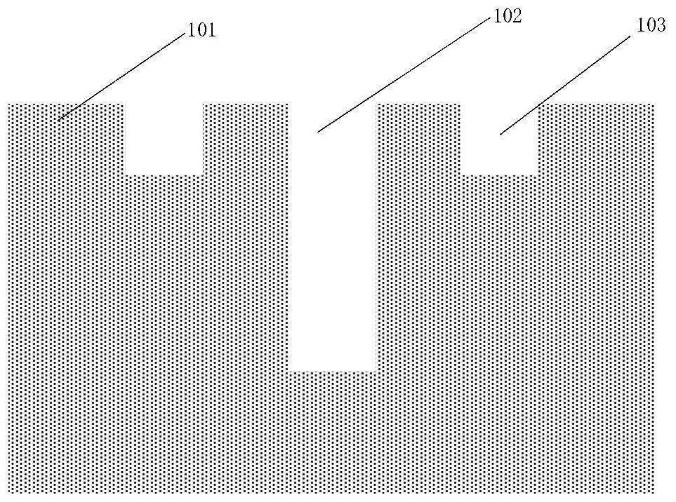
[0033] like Figure 1 to Figure 3 As shown, a method for manufacturing a three-dimensional radio frequency module based on a multi-layer heat dissipation structure specifically includes the following steps:

[0034] 101) Fabrication steps of adapter plate 101: fabricate microchannel grooves 103 and TSV holes 102 on the upper surface of adapter plate 101 by photolithography, dry or wet etching process, and the depth range of microchannel grooves 103 is 10um TSV hole 102 has a diameter ranging from 1um to 1000um and a depth ranging from 10um to 1000um. The microchannel grooves 103 are arranged on both sides of the TSV hole 102 . Silicon oxide or silicon nitride is deposited on the upper surface of the adapter plate 101 , or an insulating layer is formed by direct thermal oxidation, and the thickness of the insulating layer ranges from 10 nm to 100 um. The seed layer is made on the insulating layer by physical sputtering, magnetron sputtering or evaporation process; the thickne...

Embodiment 2

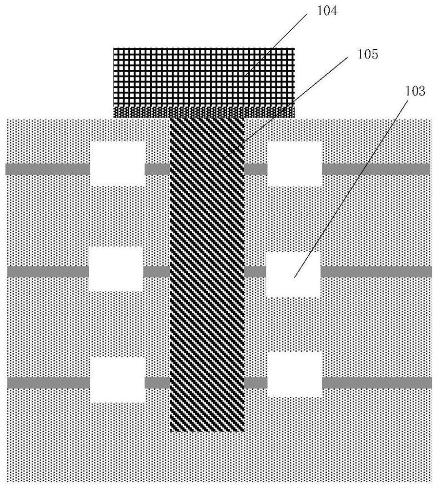
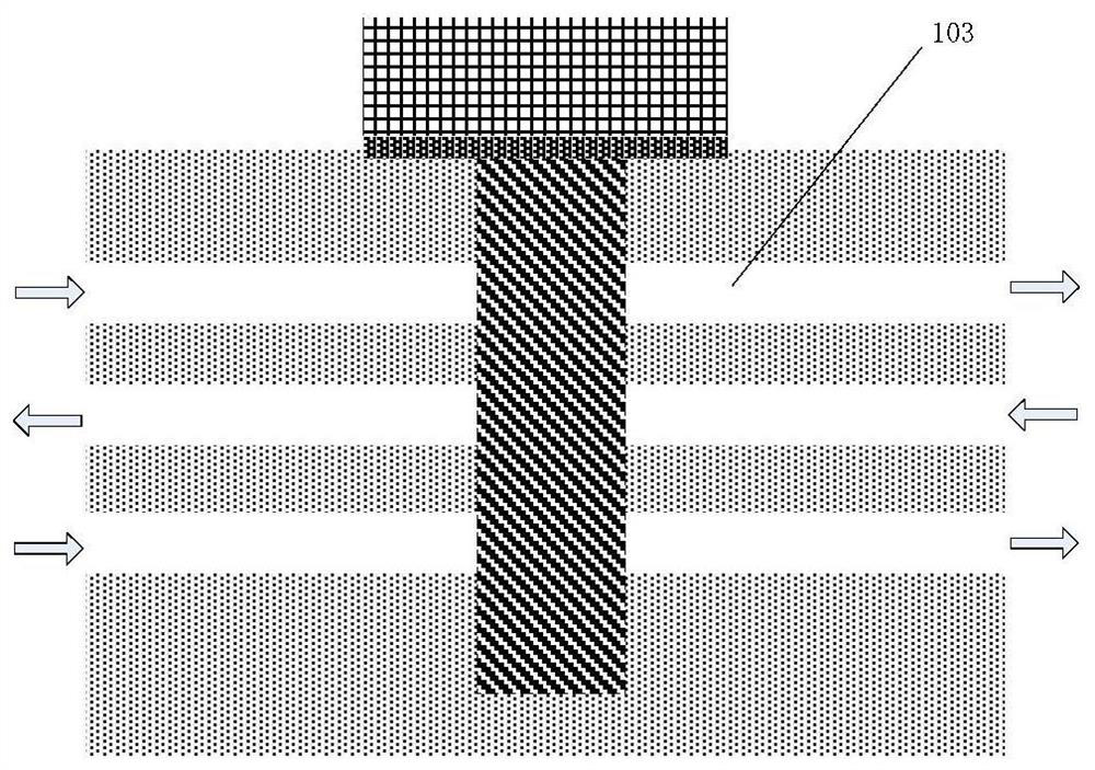
[0043] like Figure 4 to Figure 6 As shown, the difference from Embodiment 1 is that the TSV holes 102 are arranged on both sides of the micro-channel groove 103, and only the TSV holes 102 of the bottom plate are connected to each other. The TSV hole 102 is filled with a heat conducting medium 105 . A power chip 104 is soldered on the TSV hole 102 .


PUM


Abstract

The invention discloses a three-dimensional radio frequency module manufacturing method based on a multi-layer heat dissipation structure. The method specifically comprises the following steps: 101) an adapter plate manufacturing step, 102) a bottom plate manufacturing step, 103) a bonding step, and 104) a chip placement step. A heat conduction metal or a heat conduction pipeline is arranged at the bottom of a chip, the heat can be quickly conducted into a heat dissipation base, then, a plurality of layers of micro-channel liquid-phase heat dissipation channels are arranged in the heat dissipation base, and a cooling liquid in the heat dissipation channels moves in different flowing directions, so that the temperatures of the liquid in the micro-flow channels in different layers and on onesides of different chips are balanced, and the heat dissipation capacity of the micro-flow channels at the bottom of the chip tends to be consistent.

Description

technical field [0001] The invention relates to the technical field of semiconductors, more specifically, it relates to a method for manufacturing a three-dimensional radio frequency module based on a multilayer heat dissipation structure. Background technique [0002] The rapid development of electronic products is the main driving force for the evolution of packaging technology today. Miniaturization, high density, high frequency and high speed, high performance, high reliability and low cost are the mainstream development directions of advanced packaging, among which system-in-package is the most important and One of the technologies with the greatest potential to meet such high-density system integration. [0003] Among various system-in-packages, the use of silicon interposers as the substrate technology of system-in-packages provides the shortest connection distance for chip-to-chip and chip-to-PCB boards, the smallest pad size and center-to-center spacing. Advantages...

Claims


Application Information

Patent Timeline
Patent Type & Authority Applications(China)
IPC IPC(8): H01L21/48H01L23/367H01L23/473
CPCH01L21/4882H01L23/3672H01L23/473
Inventor 冯光建
Owner 浙江集迈科微电子有限公司
Why Eureka
Try Eureka