
Convolution operation architecture in CMOS image sensor

An image sensor and convolution operation technology, applied in image communication, color TV parts, TV system parts and other directions, can solve the problem of insufficient use of image sensors, achieve low power consumption, reduce data density, High frame rate effects

Active Publication Date: 2020-09-15
ZHEJIANG UNIV
View PDF5 Cites 6 Cited by
  • Summary
  • Abstract
  • Description
  • Claims
  • Application Information

AI Technical Summary

Problems solved by technology

However, these studies still have not fully utilized the characteristics of the image sensor itself. As an interface for photoelectric conversion, the pixel array itself has the function of analog storage and has the conditions to complete simple calculations.

Method used


Image

  • Convolution operation architecture in CMOS image sensor
  • Convolution operation architecture in CMOS image sensor
  • Convolution operation architecture in CMOS image sensor

Examples


Embodiment Construction

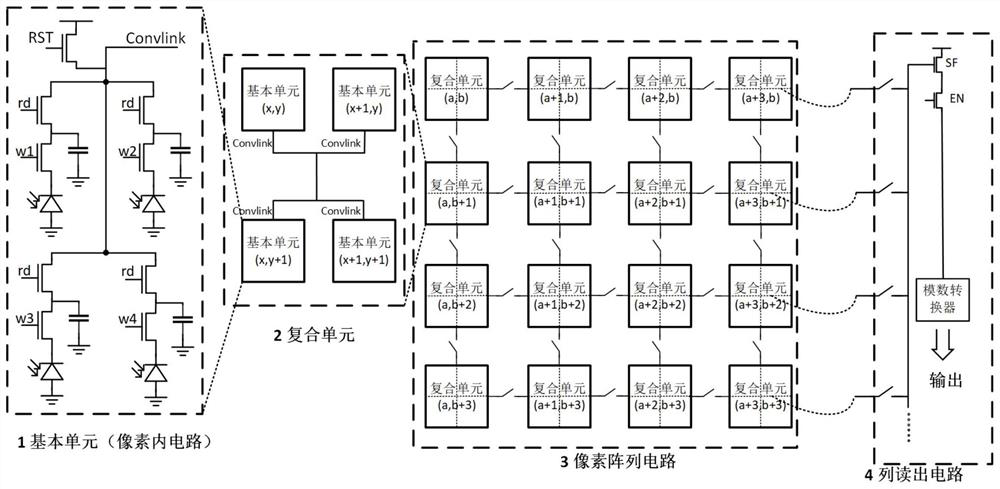
[0042] The present invention will be further described below in conjunction with the accompanying drawings and embodiments.

[0043] like Figure 4 As shown, the basic unit is mainly composed of PMOS transistor RST and four groups of identical components. The four groups of components have the same structure. The first group of components includes PMOS transistor RD1 for controlling readout and PMOS transistor W1 for controlling exposure time. 1. Photodiode D1 for photosensitive and capacitor C1 for storing charge. Pin 1 of photodiode D1 is connected to pin 2 of PMOS transistor W1. Pin 1 of PMOS transistor W1 and pin 2 of PMOS transistor RD1 are connected to pin 2 of capacitor C1. Pin 1 is connected, pin 2 of photodiode D1 and pin 2 of capacitor C1 are grounded.

[0044] The four groups of elements specifically include PMOS transistors RD1~RD4 for controlling readout, PMOS transistors W1~W4 for controlling exposure time, photodiodes D1~D4 for light sensing, and capacitors C1~C...


PUM


Abstract

The invention discloses a convolution operation architecture in a CMOS image sensor. The convolution operation architecture is provided with a pixel internal circuit serving as a basic unit for achieving light sensing and multiply-add operation, and a pixel array circuit consists of basic units and is used for achieving array convolution operation; a basic unit controls a pixel of an image, a group of elements of the basic unit represent a channel of the pixel of the image, and the conduction time of an element PMOS transistor in the basic unit is controlled by using the weight value of the channel of the pixel of the convolution kernel; charging and discharging of the capacitor are controlled through switching conduction of the PMOS transistor in the element, so that the capacitor voltageof each group of elements is controlled, and single-pixel operation control is achieved. According to the convolution operation architecture, the first-layer operation of the convolutional neural network can be completed while sensitization is performed, the first-layer operation result is converted into the digital signal to be output, the energy consumption of subsequent calculation is reduced,and the method has the characteristics of high dynamic range, high frame rate, low power consumption, variable convolution operation parameter support and the like.

Description

technical field [0001] The invention discloses a convolution operation architecture of a CMOS image sensor, and in particular relates to a convolution operation architecture of a CMOS image sensor capable of completing the convolution operation of the first layer of a convolutional neural network. Background technique [0002] In the image field, with the continuous development of machine learning technologies such as convolutional neural networks (CNN), applications such as object detection and face recognition have gradually matured, and various machine vision perception systems have been proposed. In most application scenarios, machine vision systems need to continuously shoot and work for a long time, and have strict requirements on power consumption, especially for battery-powered devices, such as field monitoring equipment and wearable devices. However, the power consumption of these systems has not been well resolved. On the one hand, deep learning algorithms often h...

Claims


Application Information

Patent Timeline
Patent Type & Authority Applications(China)
IPC IPC(8): H04N5/374H04N5/378
CPCH04N25/76H04N25/75
Inventor 黄科杰宋瑞冰沈海斌
Owner ZHEJIANG UNIV
Learn More