Display panel and preparation method thereof

A display panel and top surface technology, which is applied in semiconductor/solid-state device manufacturing, electrical components, electric solid-state devices, etc., can solve problems such as current crosstalk, reduce the display effect of the display panel, and low grayscale color shift of the display screen, so as to improve Reliability, improve the display effect, reduce the effect of leakage area

Active Publication Date: 2020-09-25
YUNGU GUAN TECH CO LTD
View PDF11 Cites 3 Cited by
  • Summary
  • Abstract
  • Description
  • Claims
  • Application Information

AI Technical Summary

Problems solved by technology

Therefore, the OLED display device in the prior art has the problem of current crosstalk between adjacent light-emitting elements, which in turn causes the problem of low grayscale color shift in the display screen and reduces the display effect of the display panel.

Method used


Image

  • Display panel and preparation method thereof
  • Display panel and preparation method thereof
  • Display panel and preparation method thereof

Examples


Embodiment Construction

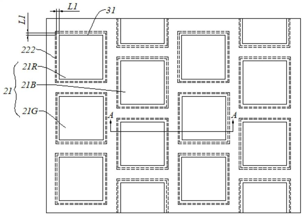
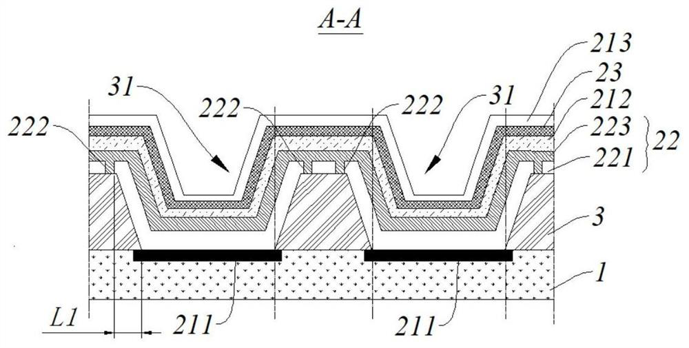
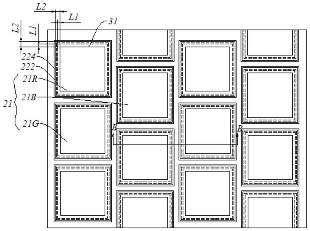
[0025] Features and exemplary embodiments of various aspects of the invention will be described in detail below. In the following detailed description, numerous specific details are set forth in order to provide a thorough understanding of the present invention. It will be apparent, however, to one skilled in the art that the present invention may be practiced without some of these specific details. The following description of the embodiments is only to provide a better understanding of the present invention by showing examples of the present invention. In the drawings and the following description, at least some well-known structures and techniques have not been shown in order to avoid unnecessarily obscuring the present invention; and, for clarity, the dimensions of some structures may have been exaggerated. Furthermore, the features, structures, or characteristics described hereinafter may be combined in any suitable manner in one or more embodiments.

[0026] In the des...


PUM


Abstract

The embodiment of the invention provides a display panel and a preparation method of the display panel. The display panel comprises an array substrate, a pixel definition layer and a first carrier layer; the pixel definition layer is located on the array substrate; the pixel definition layer comprises a plurality of pixel openings distributed in an array mode; the pixel openings comprise a first opening close to one side of the array substrate and a second opening far away from one side of the array substrate; the first carrier layer is arranged on the side, deviating from the array substrate,of the pixel definition layer; a plurality of breaking parts are arranged on the first carrier layer; the minimum distance between the orthographic projection of the breaking parts on the array substrate and the orthographic projection of the first openings on the array substrate is a first distance L1, and meets the following condition that: L1 is larger than 0 and smaller than or equal to 2 microns. According to the display panel and the preparation method of the display panel of the invention, a conductive path between at least part of adjacent light-emitting elements can be blocked, and the display effect of the display panel is improved.

Description

technical field [0001] The invention relates to the field of display technology, in particular to a display panel and a method for preparing the display panel. Background technique [0002] Organic light emitting diode (Organic Light Emitting Diode, OLED) display device is a kind of active light emitting display device, because of its advantages such as simple manufacturing process, low cost, high contrast, wide viewing angle, low power consumption, etc., it has become the mainstream flat panel display technology. . [0003] Multiple light-emitting elements of an OLED display device often have a common carrier layer, that is, the common carrier layer is connected to multiple light-emitting elements. When a light-emitting element is in a light-emitting state, the driving current applied to the light-emitting element can be applied to adjacent light-emitting elements along the common carrier layer to a certain extent, so that the light-emitting element that should be in a non...

Claims


Application Information

Patent Timeline
Patent Type & Authority Applications(China)
IPC IPC(8): H01L51/50H01L51/56H01L27/32H01L21/77
CPCH10K59/122H10K50/15H10K50/17H10K59/1201H10K71/00
Inventor 李梦真逄辉刘彬许瑾
Owner YUNGU GUAN TECH CO LTD
Why Eureka
Try Eureka