Pixel arrangement structure, high-precision metal mask plate and display panel
A pixel arrangement and sub-pixel technology, which is applied to semiconductor devices, electrical components, circuits, etc., can solve the problems of affecting the display effect and generating jagged edges at the edge of special-shaped images, etc.
- Summary
- Abstract
- Description
- Claims
- Application Information
AI Technical Summary
Problems solved by technology
Method used
Image
Examples
Embodiment 1
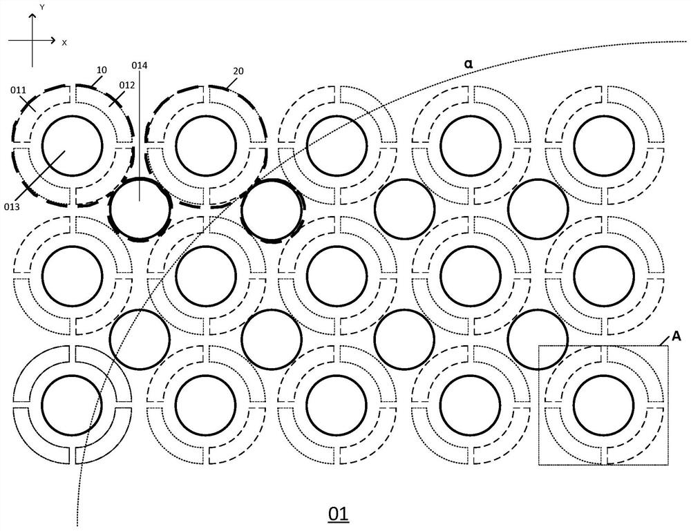
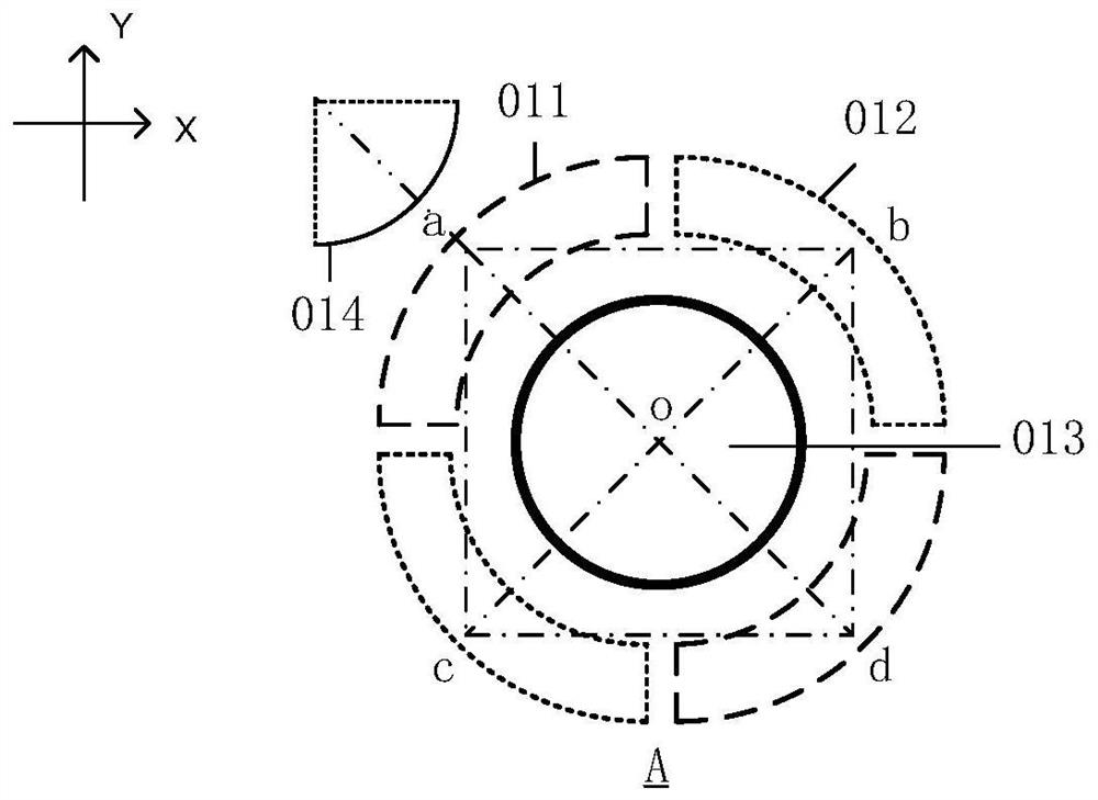
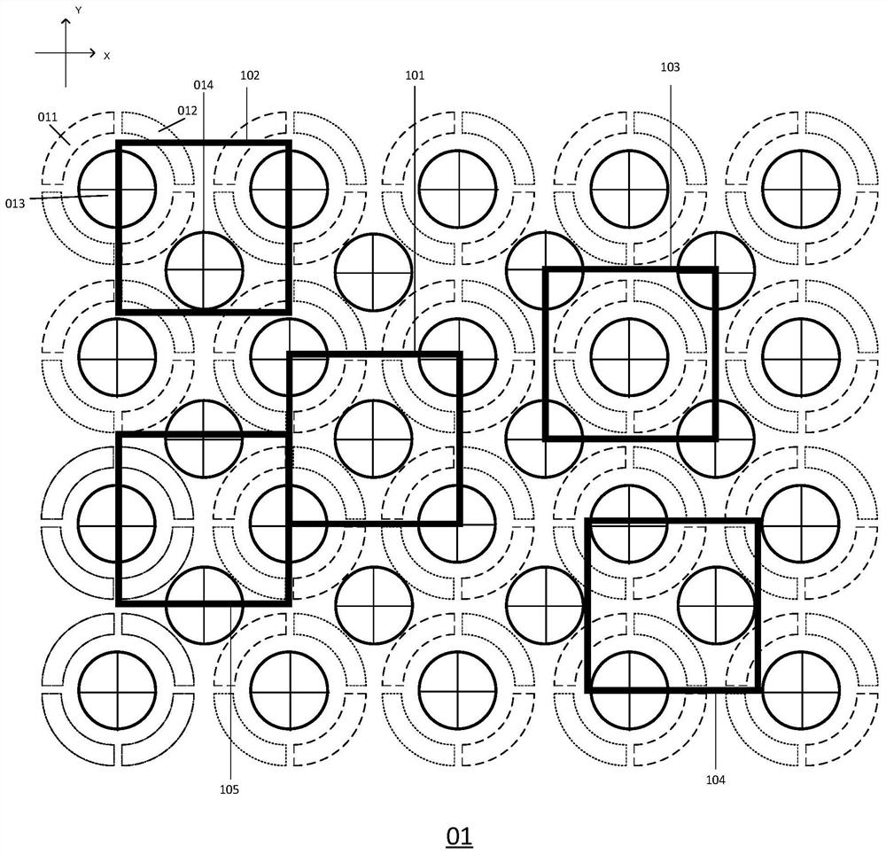
[0037] Please refer to figure 1 , the pixel arrangement structure 01 provided by the embodiment of the present invention includes a plurality of first repeating units 10 and a plurality of second repeating units 20 alternately arranged in the row direction X and the column direction Y, the first repeating units 10 and the second Each repeating unit 20 includes a first sub-pixel 011 , a second sub-pixel 012 , a third sub-pixel 013 and a fourth sub-pixel 014 . As an example, figure 1 Only a partial area of the pixel arrangement structure 01 provided in the embodiment of the present invention is intercepted; in the actual pixel arrangement structure 01, the number of first repeating units 10 may be M, where M is a positive integer not less than 1, The quantity of the second repeating unit 20 can be the same as the quantity of the first repeating unit 10, which is also M, and M is a positive integer not less than 1, and can also be one less than the quantity of the first repeat...
Embodiment 2
[0060] Please refer to Figure 4 , the pixel arrangement structure 02 provided by the embodiment of the present invention includes a plurality of first repeating units 11 and a plurality of second repeating units 21 alternately arranged in the row direction X and the column direction Y, the first repeating units 11 and the second Each repeating unit 21 includes a first sub-pixel 021 , a second sub-pixel 022 , a third sub-pixel 023 and a fourth sub-pixel 024 . As an example, Figure 4 Only a partial area of the pixel arrangement structure 02 provided in the embodiment of the present invention is intercepted; in the actual pixel arrangement structure 02, the number of first repeating units 11 may be N, where N is a positive integer not less than 1, The quantity of the second repeating unit 21 can be the same as the quantity of the first repeating unit 11, which is also N, and N is a positive integer not less than 1, and can also be one less than the quantity of the first repe...
Embodiment 3
[0089] Please refer to Figure 8 , the embodiment of the present invention provides a high-precision metal mask 03, the high-precision metal mask 03 includes openings of three shapes: the opening 311 corresponding to the second sub-pixel 012, the opening corresponding to the first sub-pixel 011 312 and an opening 313 corresponding to the third sub-pixel 013 or the fourth sub-pixel 014 . Since the third sub-pixel 013 and the fourth sub-pixel 014 have the same shape, the third sub-pixel 013 and the fourth sub-pixel 014 can share the opening 313 . As a preferred implementation manner, the shapes and positions of the openings corresponding to the sub-pixels are the same, so that during the evaporation process, the accuracy of the evaporation of the sub-pixels can be effectively improved. It can be understood that the above-mentioned openings can be set on the same mask plate, or can be set on different mask plates.
[0090] It is worth noting that, in the pixel arrangement struc...
PUM
 Abstract
Description
Claims
Application Information


