Spliced display screen

A technology of display screen and display surface, applied in the direction of instruments, identification devices, etc., can solve the problems of stitching, affecting the effect, affecting the effect of splicing display, etc.

Active Publication Date: 2020-10-13
TCL CHINA STAR OPTOELECTRONICS TECH CO LTD
View PDF6 Cites 6 Cited by
  • Summary
  • Abstract
  • Description
  • Claims
  • Application Information

AI Technical Summary

Problems solved by technology

Furthermore, when the bonding area is too large, it will affect the appearance quality of the display screen. If it is used for splicing screen applications, there will be obvious seams, which will affect the effect of splicing display.
Since polyimide, the chip-on-chip film or flexible circuit board substrate, has good resilience, it is not easy to bend, and it will also increase the seam, which will affect the effect of the splicing display

Method used


Image

  • Spliced display screen
  • Spliced display screen
  • Spliced display screen

Examples


Embodiment Construction

[0021] The following will clearly and completely describe the technical solutions in the embodiments of the application with reference to the drawings in the embodiments of the application. Apparently, the described embodiments are only some of the embodiments of the application, not all of them. Based on the embodiments in this application, all other embodiments obtained by those skilled in the art without making creative efforts belong to the scope of protection of this application.

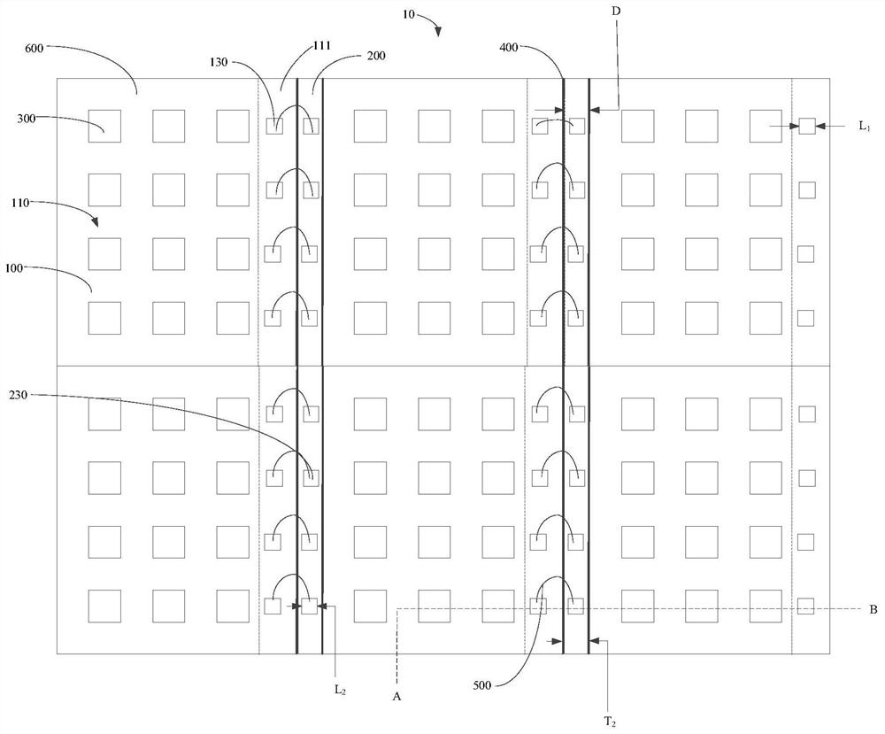
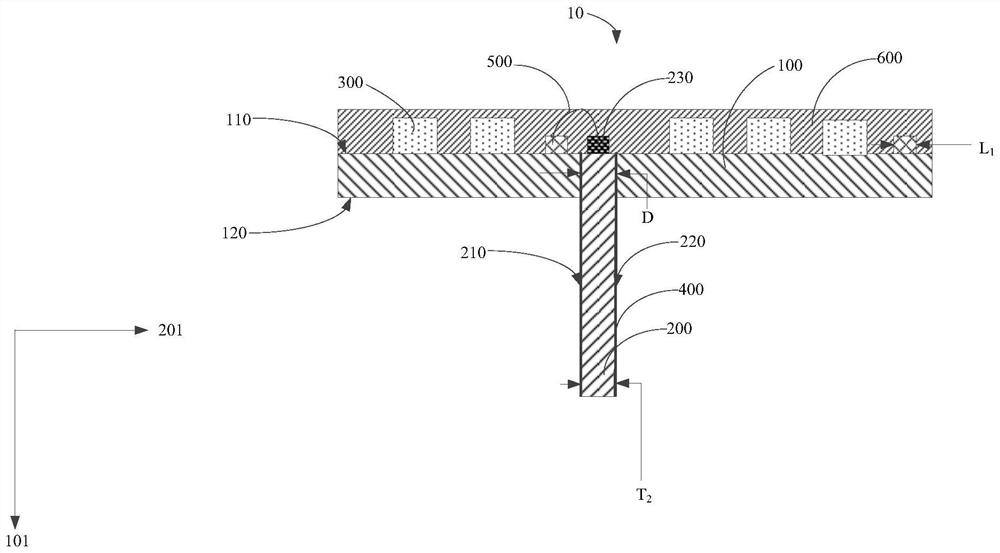
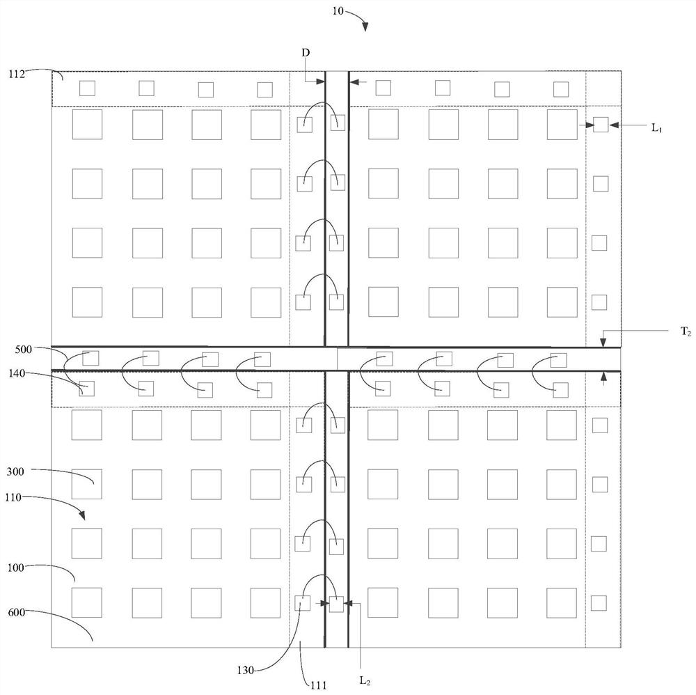
[0022] see figure 1 with figure 2 , figure 1 It is the first top view of the spliced ​​display screen provided by this application. figure 2 A cross-sectional view along line AB of the spliced ​​display screen provided for this application. The present application provides a spliced ​​display screen 10 . The spliced ​​display screen 10 includes several panels 100 and several chip-on-chip films 200 .

[0023] Each panel 100 includes a display surface 110 opposite to it and a rear surface ...


PUM

PropertyMeasurementUnit
Thicknessaaaaaaaaaa
Lengthaaaaaaaaaa

Abstract

The invention provides a spliced display screen. The spliced display screen comprises a plurality of panels and a plurality of chip-on-films. Each panel comprises a display surface and a back surfacewhich are oppositely arranged, and the direction from the display surface to the back surface is a first direction. Each chip-on-film comprises a first surface and a second surface which are oppositely arranged, and the direction from the first surface to the second surface is a second direction. One chip-on-film is clamped between every two adjacent panels. The first direction is perpendicular tothe second direction. One chip-on-film is clamped between every two adjacent panels, so that the space occupied by insufficient bending of the chip-on-films is reduced, the width of the bonding areais reduced, and the splicing seam between every two adjacent panels is reduced.

Description

technical field [0001] The present application relates to the field of display technology, in particular to a spliced ​​display screen. Background technique [0002] At present, traditional display screens need to input the signals required by the panel into the panel through the module process of bonding film on chip or flexible circuit board. Because of the panel design, it is usually necessary to bundle the in-plane signal lines through the fan-shaped area first, concentrate them in a small binding area, and then bind the chip-on-chip or flexible circuit board to the binding area. On the printed circuit board Form an electrical connection with the glass substrate, so that the width of the bonding area is usually large. Furthermore, if the bonding area is too large, it will affect the appearance quality of the display screen. If it is used for splicing screens, there will be obvious seams, which will affect the effect of splicing display. Since polyimide, the chip-on-chi...

Claims


Application Information

Patent Timeline
IPC IPC(8): G09F9/302G09F9/33
CPCG09F9/302G09F9/3026G09F9/33
Inventor 向昌明
Owner TCL CHINA STAR OPTOELECTRONICS TECH CO LTD
Why Eureka
Try Eureka