Photosensitive pixel module, image sensor and electronic device

A technology of photosensitive pixels and circuits, applied in circuits, electrical components, electric solid-state devices, etc., can solve the problems of low proportion of photosensitive pixel unit area, unfavorable imaging quality, improvement, etc., to improve photon sensitivity and imaging quality, reduce The effect of area, increased proportion and fill factor

Pending Publication Date: 2020-10-13
GUANGDONG OPPO MOBILE TELECOMM CORP LTD
View PDF7 Cites 7 Cited by
  • Summary
  • Abstract
  • Description
  • Claims
  • Application Information

AI Technical Summary

Problems solved by technology

At present, due to problems such as the structure of the pixel sensing unit, the area ratio of the photosensitive pixel unit per unit area in the image sensor is relatively low, which is not conducive to the improvement of imaging quality.

Method used


Image

  • Photosensitive pixel module, image sensor and electronic device
  • Photosensitive pixel module, image sensor and electronic device
  • Photosensitive pixel module, image sensor and electronic device

Examples


Embodiment Construction

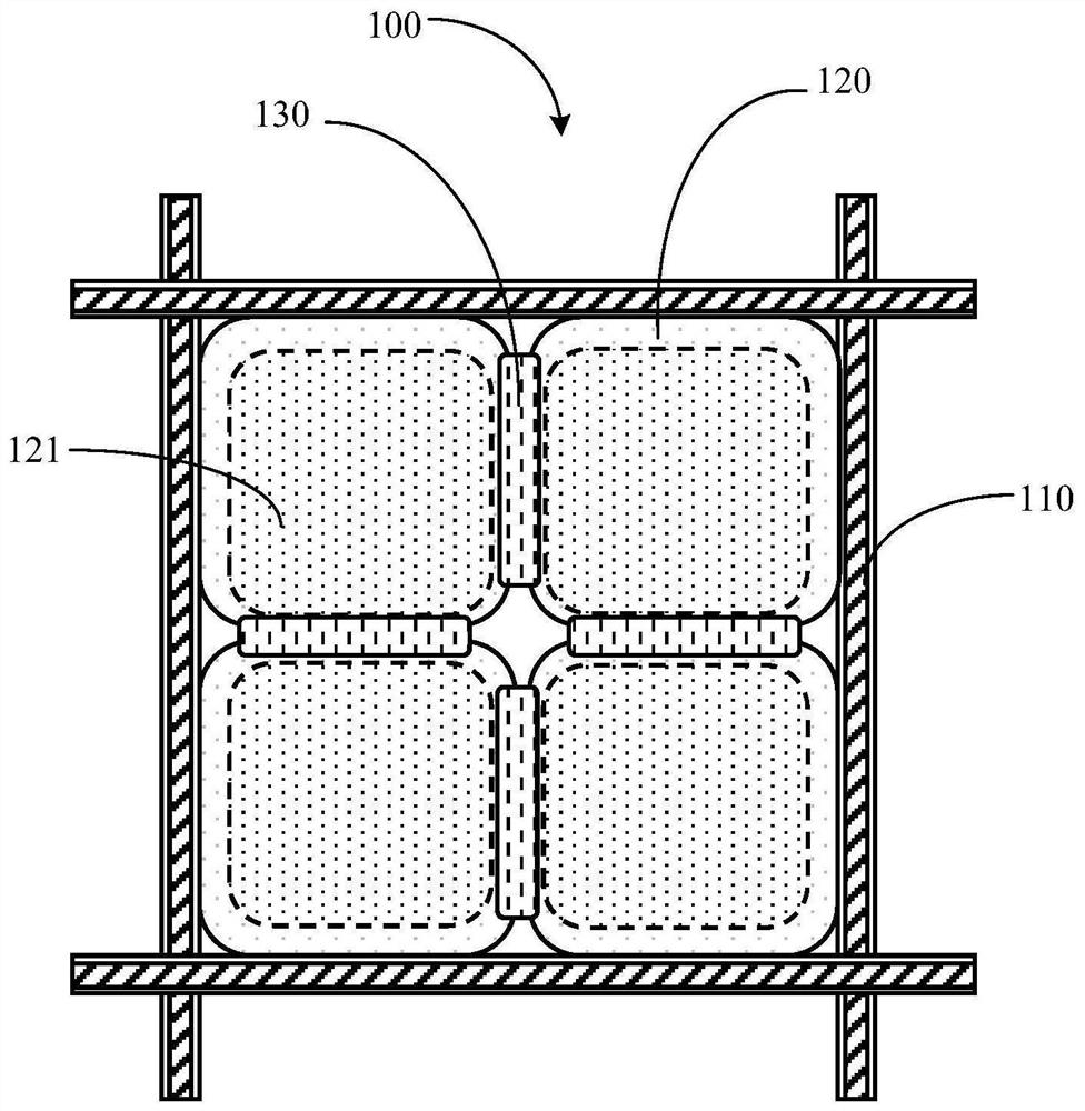
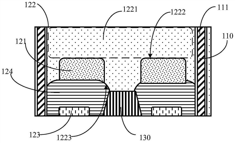
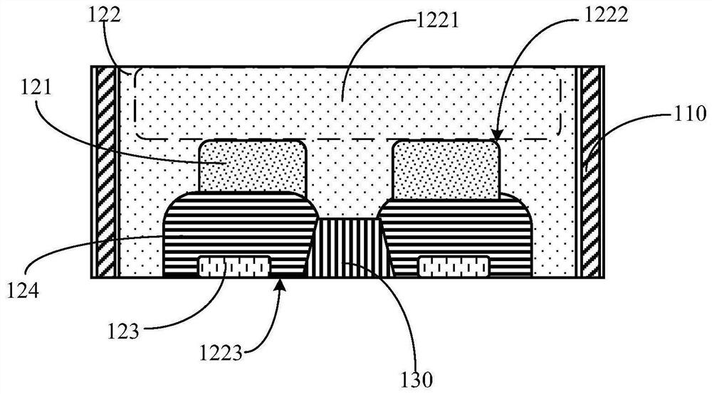
[0023] Example embodiments will now be described more fully with reference to the accompanying drawings. Example embodiments may, however, be embodied in many forms and should not be construed as limited to the embodiments set forth herein; rather, these embodiments are provided so that this disclosure will be thorough and complete, and will fully convey the concept of example embodiments to those skilled in the art. The same reference numerals in the drawings denote the same or similar structures, and thus their detailed descriptions will be omitted.

[0024] Although relative terms such as "upper" and "lower" are used in this specification to describe the relative relationship of one component of an icon to another component, these terms are used in this specification only for convenience, for example, according to the description in the accompanying drawings directions for the example described above. It will be appreciated that if the illustrated device is turned over so...


PUM

PropertyMeasurementUnit
thicknessaaaaaaaaaa

Abstract

The invention relates to a photosensitive pixel module, an image sensor and an electronic device. The photosensitive pixel module comprises a protection ring, a plurality of photosensitive pixel unitsand shallow trench isolation, and the plurality of photosensitive pixel units are arranged in the protection ring. The shallow slot isolation is arranged between any two adjacent photosensitive pixelunits in the plurality of photosensitive pixel units. A plurality of photosensitive pixel units are arranged in a protection ring. Shallow slot isolation is arranged between any two adjacent photosensitive pixel units in the plurality of photosensitive pixel units for isolation. The photosensitive pixel units share the protection ring, so that the area occupied by the protection ring is reduced,the proportion and the filling factor of the photosensitive pixel units in unit area are increased, and the photon sensitivity and the imaging quality of the image sensor are improved.

Description

technical field [0001] The present disclosure relates to the technical field of electronic equipment, in particular, to a photosensitive pixel module, an image sensor and electronic equipment. Background technique [0002] In an image sensor, light signals are usually converted into electrical signals through photosensitive pixel units, and a plurality of photosensitive pixel units are distributed in an array in the image sensor. Generally, the higher the area ratio of the photosensitive pixel units per unit area of ​​the image sensor, the higher the imaging quality of the image sensor. At present, due to problems such as the structure of the pixel sensing unit, the area ratio of the photosensitive pixel unit per unit area in the image sensor is relatively low, which is not conducive to the improvement of imaging quality. [0003] It should be noted that the information disclosed in the above background section is only for enhancing the understanding of the background of th...

Claims


Application Information

Patent Timeline
Patent Type & Authority Applications(China)
IPC IPC(8): H01L27/146
CPCH01L27/14618H01L27/1463H01L27/14636H01L27/14634H01L27/14627
Inventor 张学勇
Owner GUANGDONG OPPO MOBILE TELECOMM CORP LTD
Why Eureka
Try Eureka