

Method and system for reducing erase interference and erase time, storage medium and terminal
A technology of erasing time and over-erasing, applied in the system, a method of reducing erasing interference and erasing time, storage media and terminal fields, can solve the problem of increasing erasing time, to reduce erasing time, The effect of reducing erasure interference and meeting the requirements of product use
- Summary
- Abstract
- Description
- Claims
- Application Information
AI Technical Summary
Problems solved by technology
Method used
Image

Examples
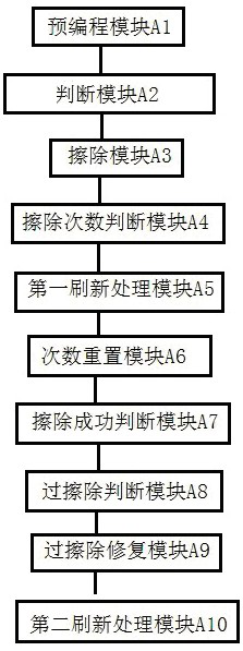
Embodiment 1
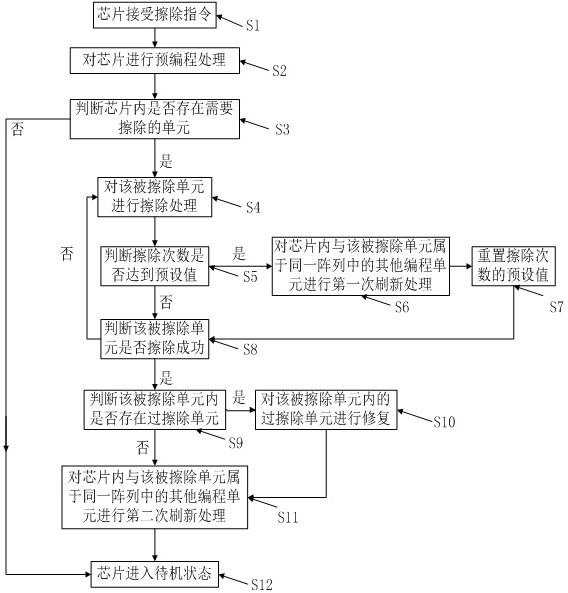
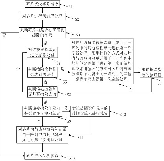
[0080] In said S6, the first refresh process is performed on other programming units in the chip that belong to the same array as the erased unit by sampling inspection:
[0081] s62-1: Randomly extract at least one other storage unit in the chip that belongs to the same array as the erased unit and judge whether the extracted storage unit is an erasing unit or a programming unit. If it is an erasing unit, jump to S7. If it is a programming unit, jump to s62-2;
[0082] s62-2: Refresh and program other memory cells in the chip that belong to the same array as the erased cell, and jump to S7.
[0083] In some specific embodiments, because the randomness is relatively large in the way of random extraction, in order to reduce the reduction of chip reliability caused by randomness, the S6 specifically includes the following steps:
[0084] s62-1: Randomly extract at least one (one or more) other storage units in the chip that belong to the same array as the erased unit and judge ...
Embodiment 2
[0089] In said S6, the first refresh process is performed on other programming units in the chip that belong to the same array as the erased unit in a cyclic manner:
[0090] s63-1: Extract the current storage unit according to the preset extraction arrangement rule and the preset number of storage units and then the last extracted unit, and judge whether the currently extracted storage unit is an erasing unit or a programming unit, if it is an erasing unit Then jump to S7, if it is a programming unit, then jump to s63-2;
[0091] s63-2: Refresh and program the currently extracted memory cells, and jump to S7.
[0092] Among them, the preset extraction arrangement can be in order, for example, the sector numbered 1, the sector numbered 2 and the sector numbered 3 were extracted last time, and the sector numbered 4 is extracted next time. , the sector numbered 5 and the sector numbered 6..., or the sector with an odd number was extracted last time, and the sector with an even ...
PUM
 Abstract
Description
Claims
Application Information