Storage device and semiconductor apparatus

Inactive Publication Date: 2007-07-05
SONY CORP
View PDF3 Cites 3 Cited by
  • Summary
  • Abstract
  • Description
  • Claims
  • Application Information

AI Technical Summary

Benefits of technology

[0041] Accordingly, it is desirable to provide a storage device and a semiconductor apparatus capable of reducing power consumption when erasing is performed on a memory cell and reducing an erasing time for the memory cell.
[0046] According to the storage device and the semiconductor apparatus, power consumption can be reduced, and erasing on a memory array can be performed at high speed.

Problems solved by technology

Thus, a large amount of time is necessary for erasing.
However, as the capacity of the storage device increases, the power consumption necessary for batch erasing enormously increases.
Thus, it is, in effect, difficult to perform batch erasing.

Method used


Image

  • Storage device and semiconductor apparatus
  • Storage device and semiconductor apparatus
  • Storage device and semiconductor apparatus

Examples


Embodiment Construction

[0056] Embodiments of the present invention will be described with reference to the drawings.

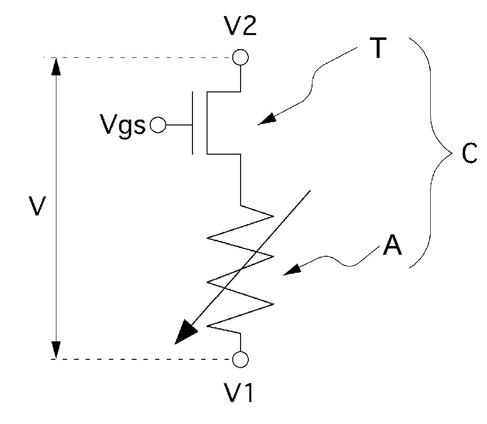
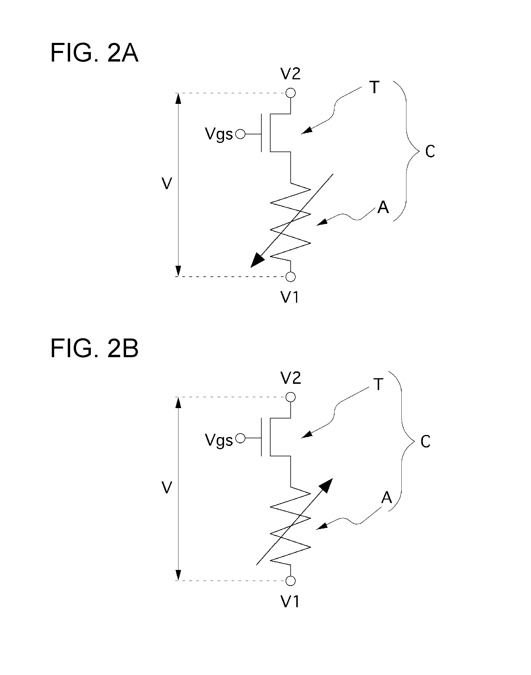
[0057] In the embodiments of the present invention, a storage device includes a resistance change storage element (hereinafter, referred to as a memory element) used for a memory cell.

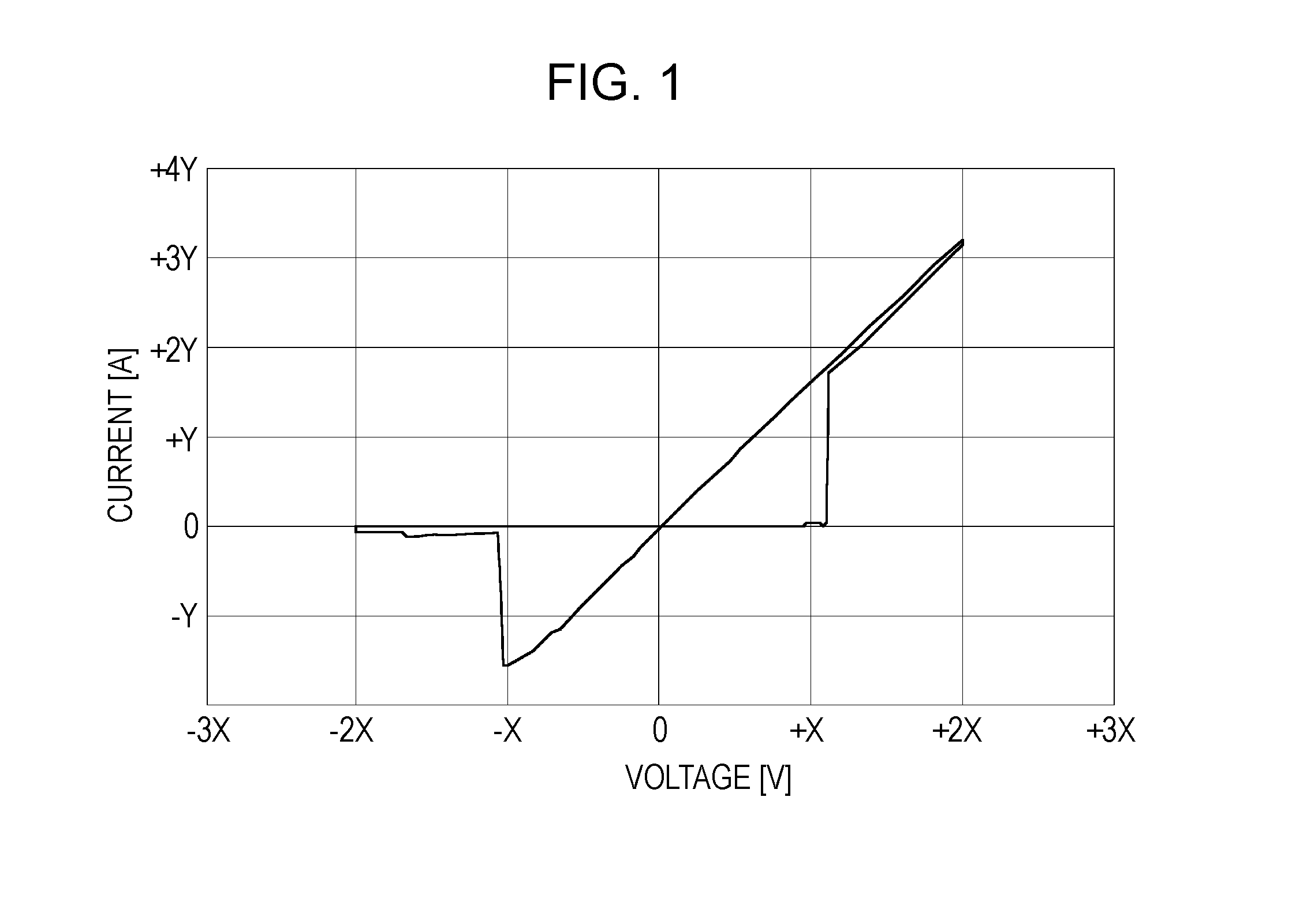
[0058]FIG. 1 is a graph showing a current-voltage (I-V) change of a memory element used in a storage device according to an embodiment of the present invention.

[0059] As a memory element having the I-V characteristic shown in FIG. 1, for example, a storage element including a storage layer that is sandwiched between a first electrode and a second electrode (for example, between a lower electrode and an upper electrode) and that is made of an amorphous thin film, such as a rare-earth oxide film or the like, is used.

[0060] In the initial state, the memory element has a high resistance (for example, 1 MΩ or more), and a current does not flow easily. Referring to FIG. 1, when a voltage of +1.1X V (for example, ...


PUM


Abstract

A storage device includes memory cells disposed in a matrix. The memory cells each include a storage element whose resistance changes from a higher state to a lower state when an electric signal of a first threshold level or higher is applied and whose resistance changes from the lower state to the higher state when an electric signal of a second threshold level or higher whose polarity is different from the polarity of the electric signal of the first threshold level or higher is applied, and a circuit element connected in series with the storage element. In a state in which an erasing voltage is applied to at least one memory cell on which erasing is currently being performed, after the lapse of a predetermined time from the application, an erasing voltage is applied to at least one memory cell on which erasing is to be next performed.

Description

CROSS REFERENCES TO RELATED APPLICATIONS [0001] The present invention contains subject matter related to Japanese Patent Application JP 2005-162307 filed in the Japanese Patent Office on Jun. 2, 2005, the entire contents of which are incorporated herein by reference. BACKGROUND OF THE INVENTION [0002] 1. Field of the Invention [0003] The present invention relates to storage devices and semiconductor apparatuses, and more particularly, to a storage device and a semiconductor apparatus that include memory cells each including a storage element storing and holding information in accordance with an electric resistance state. [0004] 2. Description of the Related Art [0005] In information apparatuses, such as computers, high-density dynamic random access memories (DRAMs) with high operation speed are widely used as random access memories (RAMs). [0006] However, since DRAMs are volatile memories, which lose information when the power is turned off, nonvolatile memories, which hold informat...

Claims


Application Information

Patent Timeline
IPC IPC(8): G11C11/00
CPCG11C11/22G11C13/0004G11C13/0007G11C13/0011G11C2213/79G11C13/0069G11C13/0097G11C2213/31G11C13/0061G11C11/16
Inventor MORI, HIRONOBUHACHINO, HIDENARIOKAZAKI, NOBUMICHI
Owner SONY CORP
Why Eureka
Try Eureka