Flash chip and erasing method thereof

A chip and area technology, applied in the field of memory, can solve problems such as prolonging erasing time, increasing erasing operation time overhead, reducing erasing efficiency, etc., to achieve the effect of reducing overhead, improving erasing performance, and increasing erasing speed

Active Publication Date: 2015-09-02
GIGADEVICE SEMICON (BEIJING) INC
View PDF5 Cites 3 Cited by
  • Summary
  • Abstract
  • Description
  • Claims
  • Application Information

AI Technical Summary

Problems solved by technology

However, in the prior art, the erasing repair operation performed to eliminate erasing interference prolongs the erasing time and increases the time overhead of the erasing operation, thereby reducing the erasing efficiency

Method used


Image

  • Flash chip and erasing method thereof
  • Flash chip and erasing method thereof
  • Flash chip and erasing method thereof

Examples


Embodiment Construction

[0042] The present invention will be described in more detail and complete below in conjunction with the accompanying drawings and specific embodiments. It should be understood that the specific embodiments described here are only used to explain the present invention, but not to limit the present invention. In addition, it should be noted that, for the convenience of description, only parts related to the present invention are shown in the drawings but not all content.

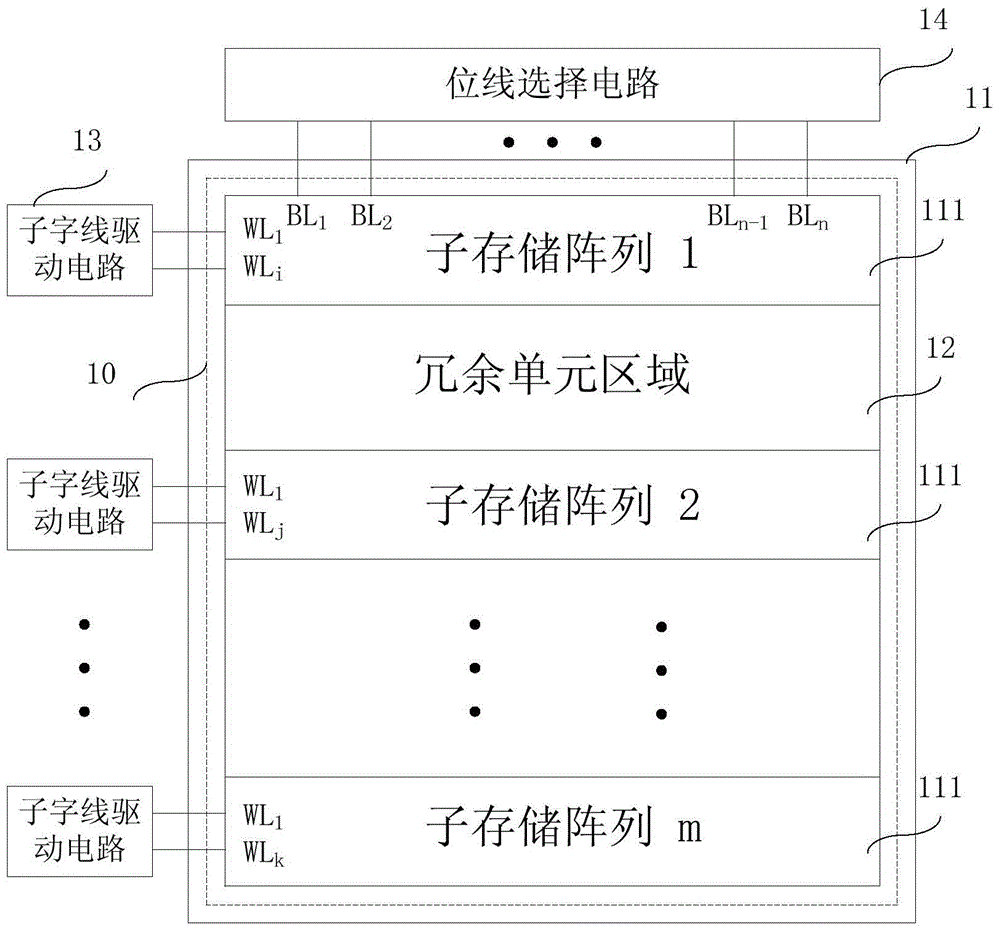
[0043] figure 1 Shown is a schematic structural diagram of the FLASH chip in Embodiment 1 of the present invention.

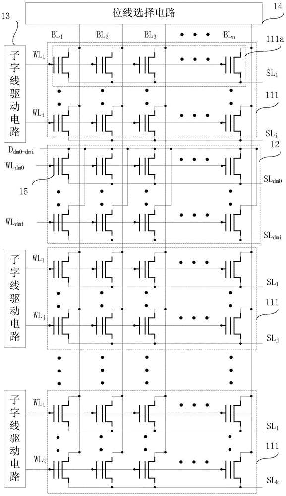
[0044] Figure 1a Shown is a schematic diagram of the distribution structure of storage units in the FLASH chip storage array in Embodiment 1 of the present invention.

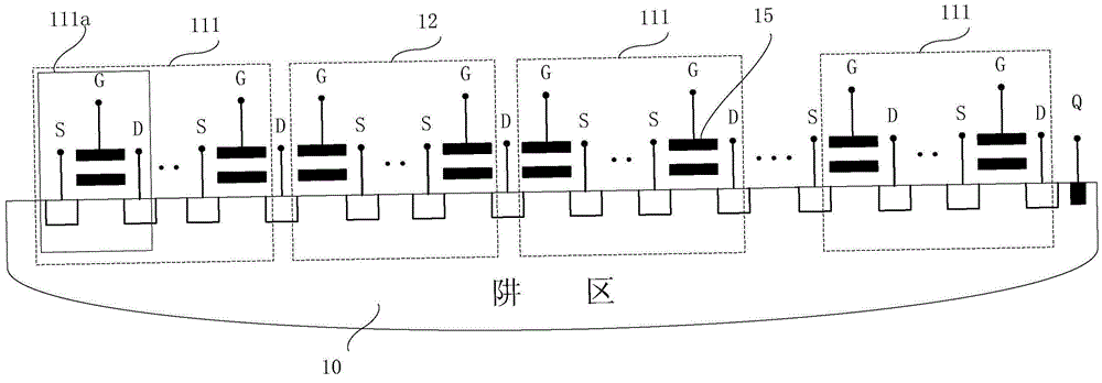
[0045] Figure 1b Shown is a schematic cross-sectional structure diagram of the distribution of memory cells in the FLASH chip memory array in Embodiment 1 of the present invention.

[0046] refer to figure 1 , Figure ...


PUM


Abstract

The invention relates to the technical field of memories and particularly relates to a flash chip and an erasing method thereof. The flash chip comprises a memory array, m word line driving sub-circuits and a bit line selecting circuit, wherein the memory array comprises m memory subarrays and a redundancy unit zone; the m memory subarrays are formed in one well region; the redundancy unit zone is formed between two adjacent memory subarrays; during erasing, a drain electrode of a memory unit in the redundancy unit zone is suspended in midair; the m word line driving sub-circuits are respectively connected to the m memory subarrays; each word line driving sub-circuit provides driving signal to the memory subarray connected to the corresponding word line driving sub-circuit; and the bit line selecting circuit provides a plurality of bit lines, is connected to drain electrodes of memory units of the memory subarrays in each row of the memory array and is used for selecting the memory units in the memory subarrays. Erasing performance of the flash chip provided by embodiments is improved and erasing time of the flash chip is shortened, thus increasing the erasing efficiency.

Description

technical field [0001] The invention relates to the technical field of memory, in particular to a FLASH chip and an erasing method using the FLASH chip. Background technique [0002] In the prior art, when flash memory (Flash Memory) is erased, a positive high voltage is applied to the well region where the memory cell is located in the pre-erased area and the source (S) of the pre-erased memory cell, and a negative high voltage is applied to the control gate (CG), and Floating drain (D); in this way, the applied positive and negative high voltages form a voltage difference between the floating gate (FG) and source of the memory cell, creating a tunnel effect that allows charges in the floating gate to flow to the source , and then change the threshold voltage of the memory cell to realize erasing of the pre-erased memory cell. At the same time, when erasing, the same positive high voltage is applied to the source of the memory cells in the non-erased area in the same well ...

Claims


Application Information

Patent Timeline
Patent Type & Authority Applications(China)
IPC IPC(8): G11C16/14
Inventor 胡洪陈建梅
Owner GIGADEVICE SEMICON (BEIJING) INC
Why Eureka
Try Eureka