Erasing method and device of memory unit

A memory cell and erasing voltage technology, applied in the storage field, can solve problems such as slowing down the erasing speed, achieve the effect of reducing the impact and improving the erasing performance

Inactive Publication Date: 2018-06-01
GIGADEVICE SEMICON (BEIJING) INC
View PDF3 Cites 5 Cited by
  • Summary
  • Abstract
  • Description
  • Claims
  • Application Information

AI Technical Summary

Problems solved by technology

[0005] The invention provides a method and device for erasing a storage unit, so as to improve the problem of slow erasing speed at low temperature and improve erasing performance

Method used


Image

  • Erasing method and device of memory unit
  • Erasing method and device of memory unit
  • Erasing method and device of memory unit

Examples


Embodiment 1

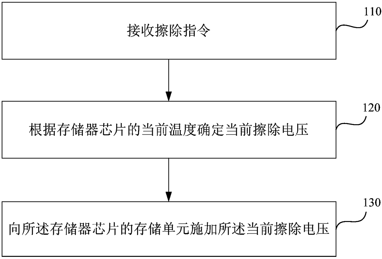
[0042] figure 2 It is a schematic flowchart of a method for erasing a memory cell provided by Embodiment 1 of the present invention. This embodiment is applicable to the case where memory cells are erased at different temperatures. see figure 2 The erasing method of the storage unit provided in this embodiment specifically includes the following steps:

[0043] 110. Receive an erase instruction.

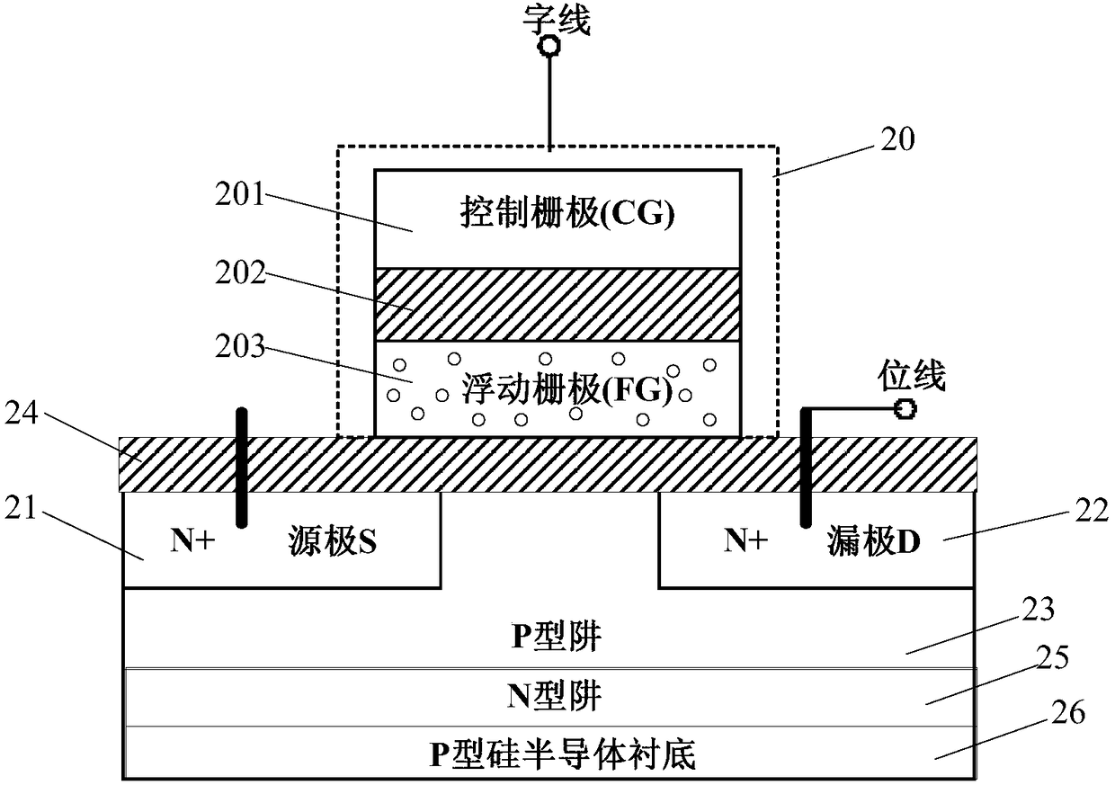
[0044] The flash chip is composed of thousands of internal storage units, each storage unit stores one bit of data, multiple storage units form a page, multiple pages form a block, and multiple blocks form a storage unit array. Special physical structure, in nor flash / nand flash, the erase operation is performed in units of blocks; the storage unit array is composed of a plurality of storage unit blocks, and the storage unit block is composed of a plurality of storage unit pages, and the storage unit A cell page consists of multiple memory cells connected in rows and columns. I...

Embodiment 2

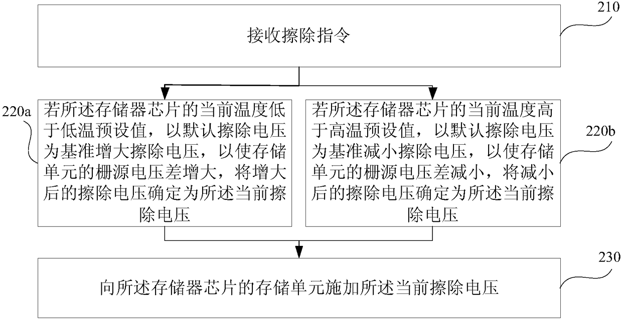
[0056] image 3 It is a schematic flow chart of a memory cell erasing method provided by Embodiment 2 of the present invention. This embodiment is further optimized on the basis of Embodiment 1, and is especially applicable when the temperature change of the memory chip causes the erasing speed to become slow or slow down. In the fast case, the advantage of optimization is that when the temperature of the memory chip is lower than the low temperature preset value or higher than the high temperature preset value, the erasing voltage matching the temperature is determined to ensure the erasing speed and improve over-erase erase phenomenon and improve erase performance. For details, please refer to image 3 , the method specifically includes the following steps:

[0057] 210. Receive an erase instruction.

[0058] 220a. If the current temperature of the memory chip is lower than the low temperature preset value, increase the erasing voltage based on the default erasing voltage...

Embodiment 3

[0066] Figure 4 It is a schematic structural diagram of an erasing device for a storage unit provided in Embodiment 3 of the present invention, and the device specifically includes:

[0067] receiving module 410, determining module 420 and applying module 430;

[0068] Wherein, the receiving module 410 is used to receive the erasing instruction; the determining module 420 is used to determine the current erasing voltage according to the current temperature of the memory chip; the applying module 430 is used to apply the current erasing voltage to the storage unit of the memory chip. In addition to voltage.

[0069] Further, the device may further include a detection module, configured to detect the current temperature of the memory chip through a temperature sensor before the current erasing voltage is determined according to the current temperature of the memory chip.

[0070] Further, the determining module 420 may include:

[0071] An increasing unit, configured to incr...


PUM


Abstract

The invention discloses an erasing method and device of a memory unit. The method comprises the steps as follows: receiving an erasing instruction; determining the current erasing voltage according tothe current temperature of a memory chip; applying the current erasing voltage to the memory unit of the memory chip. According to the erasing method of the memory unit, by means of the technical means that the current erasing voltage is determined according to the current temperature of the memory chip and current erasing voltage is applied to the memory unit of the memory chip, the problem thatthe erasing speed at the low temperature decreases is solved, the problem of over-erasure caused by ultrahigh erasing speed at the high temperature is solved, and the erasing performance is improved.

Description

technical field [0001] Embodiments of the present invention relate to the field of storage technology, and in particular to a method and device for erasing a storage unit. Background technique [0002] Non-volatile flash memory (nor flash / nand flash) is a very common memory chip, which has the advantages of random access memory (RAM) and read-only memory (Read-Only Memory, ROM). It will not be lost. It is a memory that can be electrically erased and written in the system. At the same time, its high integration and low cost make it the mainstream of the market. [0003] In a flash chip, a memory cell can be regarded as a metal-oxide-semiconductor field-effect transistor (Metal-Oxide-Semiconductor Field-Effect Transistor, MOSFET). figure 1 It is a common MOSFET structure diagram, including a gate 20, a source 21, a drain 22, a P-type well 23, an N-type well 25, a P-type silicon semiconductor substrate 26, and a tunnel oxide layer 24. The connection is: the P-type silicon sem...

Claims


Application Information

Patent Timeline
Patent Type & Authority Applications(China)
IPC IPC(8): G11C16/14G11C16/30
CPCG11C16/14G11C16/30
Inventor 胡洪张建军卜尔龙
Owner GIGADEVICE SEMICON (BEIJING) INC
Why Eureka
Try Eureka