Display device and driving method for same
一种显示装置、驱动晶体管的技术,应用在静态指示器、仪器、半导体器件等方向,能够解决偏差显示品质、易产生偏差、降低等问题,达到防止亮度偏差、电压大小的变化小的效果
- Summary
- Abstract
- Description
- Claims
- Application Information
AI Technical Summary
Problems solved by technology
Method used
Image

Examples
no. 1 approach
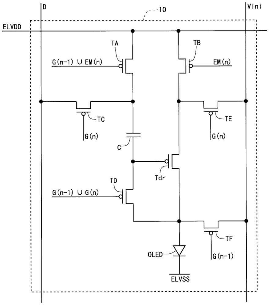
[0069]
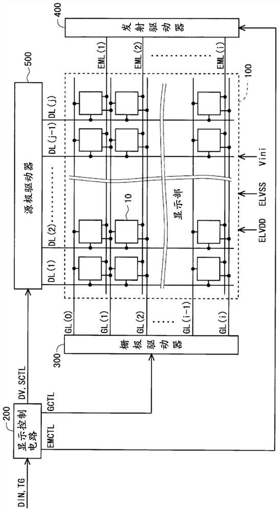
[0070] figure 2 It is a block diagram showing the overall configuration of the organic EL display device of the first embodiment. This organic EL display device includes a display section 100 , a display control circuit 200 , a gate driver 300 , an emission driver 400 , and a source driver 500 . In addition, for example, the gate driver 300 and the emission driver 400 are provided inside the organic EL panel, and the display control circuit 200 and the source driver 500 are provided on a substrate outside the organic EL panel, in addition to the display unit 100 .
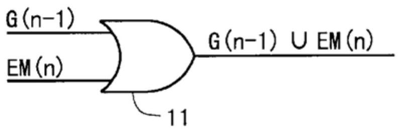
[0071] In the display unit 100 , (i+1) scanning signal lines GL( 0 ) to GL(i) and j data signal lines DL( 1 ) to DL(j) orthogonal to these are provided. Also, in the display unit 100, i light emission control lines EML(1) are provided in one-to-one correspondence with the i scanning signal lines GL(1) to GL(i) other than the scanning signal line GL(0). )~EML(i). In the display unit 100 , the scanning...
no. 2 approach
[0117] The second embodiment will be described. In addition, since the overall configuration is the same as that of the first embodiment, description thereof will be omitted.
[0118]
[0119] while referring to Figure 9 , the configuration of the pixel circuit 10 of this embodiment will be described. This pixel circuit 10, such as Figure 9 As shown, it includes a light emitting element OLED, eight transistors (driving transistor Tdr, first power supply control transistor TA1, second power supply control transistor TA2, light emission control transistor TB, first write control transistor TC, threshold voltage compensation transistor TD, the second write control transistor TE, and the initialization transistor TF), a data holding capacitor C. Hereinafter, description will be given mainly on points different from the first embodiment, and description on points similar to the first embodiment will be appropriately omitted.
[0120] In the first embodiment, one power suppl...
no. 3 approach
[0137] The third embodiment will be described. In addition, since the overall configuration is the same as that of the first embodiment, description thereof will be omitted.
[0138]
[0139] while referring to Figure 15 , the configuration of the pixel circuit 10 of this embodiment will be described. This pixel circuit 10, such as Figure 15 As shown, it includes a light emitting element OLED, eight transistors (drive transistor Tdr, power supply control transistor TA, light emission control transistor TB, first write control transistor TC, first threshold voltage compensation transistor TD1, second threshold voltage compensation transistor TD2, the second write control transistor TE, and the initialization transistor TF), a data holding capacitor C.
[0140] In the first embodiment, a threshold voltage compensation transistor TD is provided to electrically connect between the gate terminal and the second conduction terminal of the driving transistor Tdr during the init...
PUM
 Abstract
Description
Claims
Application Information
 - R&D Engineer
- R&D Manager
- IP Professional
- Industry Leading Data Capabilities
- Powerful AI technology
- Patent DNA Extraction
Browse by: Latest US Patents, China's latest patents, Technical Efficacy Thesaurus, Application Domain, Technology Topic.
© 2024 PatSnap. All rights reserved.Legal|Privacy policy|Modern Slavery Act Transparency Statement|Sitemap