
Memory cell having a buried phase change region and method for fabricating the same

一种存储单元、存储元件的技术,应用在信息存储、静态存储器、数字存储器信息等方向,能够解决小电极结构稳定度等问题

Active Publication Date: 2010-10-27
MACRONIX INT CO LTD +1
View PDF10 Cites 4 Cited by
  • Summary
  • Abstract
  • Description
  • Claims
  • Application Information

AI Technical Summary

Problems solved by technology

[0009] Therefore, there is a need for a reliable manufacturing method of memory cells, which can be used in memory cells of high-density integrated circuit memory devices, has good control on the critical dimension of the bottom electrode, and can solve the structural stability of very small electrodes question

Method used


Image

  • Memory cell having a buried phase change region and method for fabricating the same
  • Memory cell having a buried phase change region and method for fabricating the same
  • Memory cell having a buried phase change region and method for fabricating the same

Examples


Embodiment Construction

[0076] The description of the invention that follows will refer to specific structural embodiments and methods. It is to be understood that the scope of the invention is not limited to the specific disclosed embodiments and that the invention can be practiced with other features, elements, methods and embodiments. The preferred embodiments are described to understand the present invention, but not to limit the scope of the present invention, which is defined by the claims. Those skilled in the art can understand equivalent changes of the present invention according to the subsequent description. Similar elements in various embodiments will be designated with similar reference numerals.

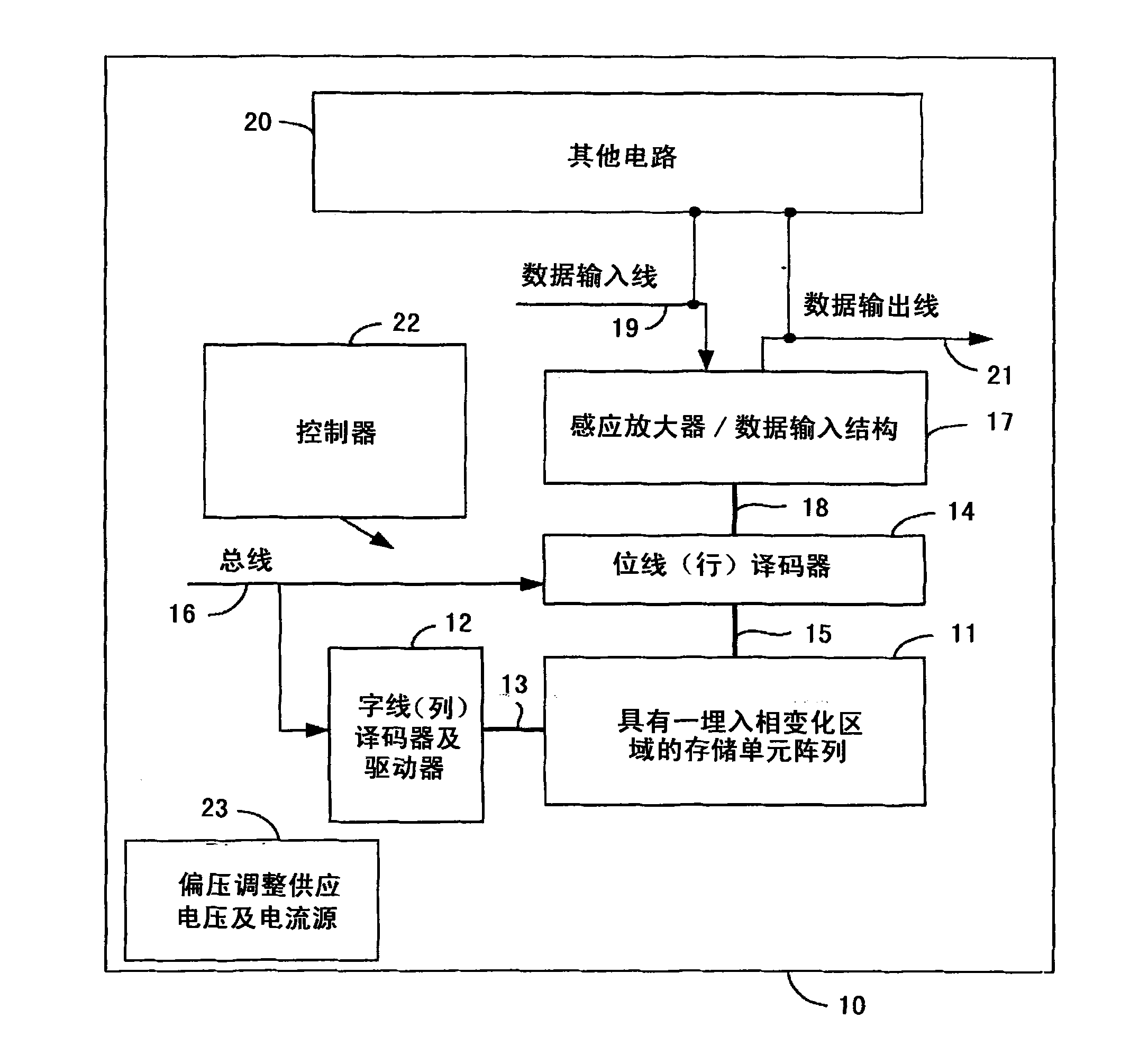
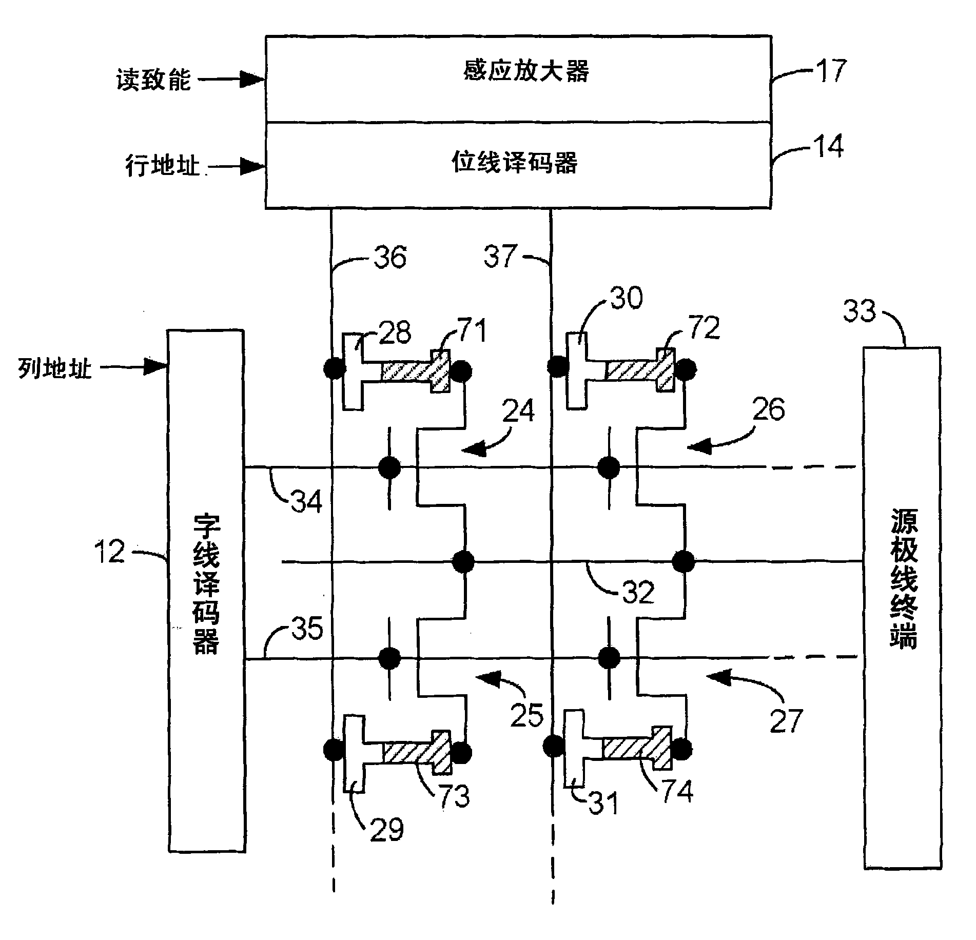
[0077] Please refer to figure 1 , which is a simplified block diagram showing an integrated circuit 10 according to an embodiment of the present invention. The integrated circuit 10 includes a memory array 11, which uses umbrella phase-change memory cells disclosed in the present invention ...


PUM


Abstract

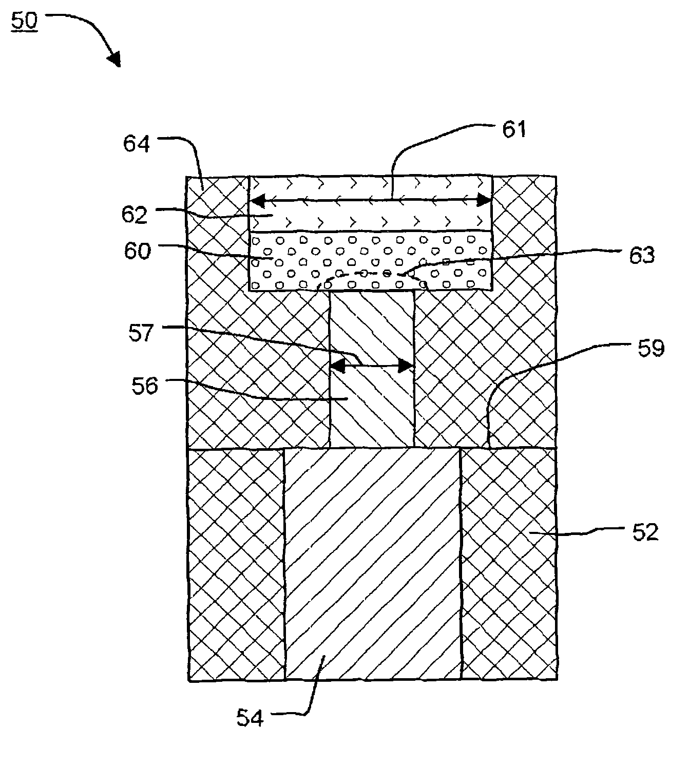
Memory cells are described along with methods for manufacturing. A memory cell as described herein includes a bottom electrode comprising a base portion and a pillar portion on the base portion, the pillar portion having a width less than that of the base portion. A dielectric surrounds the bottom electrode and has a top surface. A memory element is overlying the bottom electrode and includes a recess portion extending from the top surface of the dielectric to contact the pillar portion of the bottom electrode, wherein the recess portion of the memory element has a width substantially equal to the width of the pillar portion of the bottom electrode. A top electrode is on the memory element.

Description

technical field [0001] The present invention relates to high density memory devices using phase change based memory materials, such as chalcogenides and other programmable resistive materials, and methods of making such devices. Background technique [0002] Phase-change based memory materials, such as chalcogenides and the like, can be induced to change crystal phase by applying a current of magnitude suitable for use in integrated circuits. Generally speaking, the characteristic of the amorphous state is that its resistance is higher than that of the crystalline state, and this resistance value can be easily measured and used as an indicator. This property has sparked interest in using programmable resistive materials to form nonvolatile memory circuits that can be used for random access reading and writing. [0003] The transition from the amorphous state to the crystalline state is generally a low current step. The transition from a crystalline state to an amorphous st...

Claims


Application Information

Patent Timeline
Patent Type & Authority Applications(China)
IPC IPC(8): H01L45/00H01L27/24G11C11/56
CPCH01L27/2436G11C11/5678H01L45/06H01L45/148H01L45/143H01L45/14H01L45/1625H01L45/1666H01L27/2472H01L45/144H01L45/1641H01L45/126H01L45/1233G11C13/0004H10B63/82H10B63/30H10N70/8413H10N70/881H10N70/231H10N70/8825H10N70/884H10N70/041H10N70/061H10N70/026H10N70/8828H10N70/826
Inventor 龙翔澜林仲汉杨明亚历桑德罗·加布里埃尔·史克鲁特
Owner MACRONIX INT CO LTD
Learn More