Supercharge Your Innovation With Domain-Expert AI Agents!

LED display substrate and preparation method thereof

A technology for display substrates and base substrates, applied in electrical components, electric solid devices, circuits, etc., can solve problems such as the inability to directly prepare large-size LED display substrates and affect the display quality of LED display substrates

Pending Publication Date: 2020-10-30
BOE TECH GRP CO LTD +1
View PDF4 Cites 1 Cited by
  • Summary
  • Abstract
  • Description
  • Claims
  • Application Information

AI Technical Summary

Problems solved by technology

Usually, Micro / Mini-LED chips are transferred to the display substrate by transfer printing technology. Due to the limitation of transfer printing technology, it is impossible to directly prepare large-size LED display substrates; therefore, in the prior art, multiple small Large-sized LED display substrates are spliced ​​to form large-sized LED display substrates
[0003] At present, the signal traces in the LED display substrate are made of metal materials (such as copper) and run through the display area. Due to the high light reflectivity of the metal material, the signal traces are clearly visible in the display area, thus affecting Improve the display quality of the LED display substrate

Method used


Image

  • LED display substrate and preparation method thereof
  • LED display substrate and preparation method thereof
  • LED display substrate and preparation method thereof

Examples


Embodiment Construction

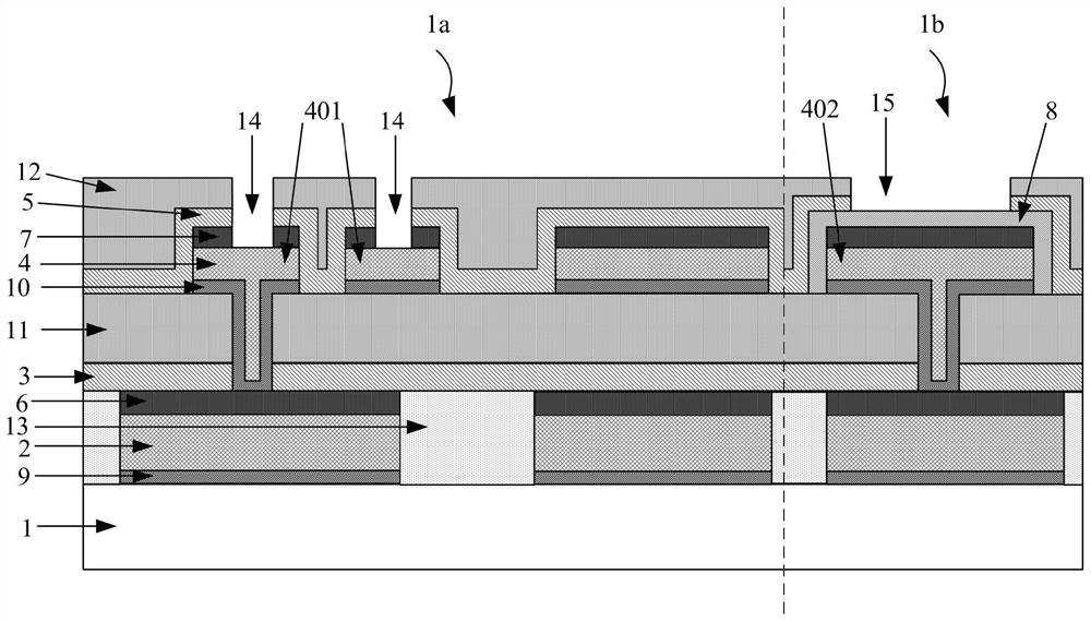
[0065] In order for those skilled in the art to better understand the technical solutions of the present invention, an LED display substrate and a manufacturing method thereof provided by the present invention will be described in detail below with reference to the accompanying drawings.

[0066] figure 1 A schematic structural diagram of an LED display substrate provided by an embodiment of the present disclosure, as shown in figure 1 As shown, the LED display substrate includes: a base substrate 1 , a first metal conductive layer pattern 2 , a first passivation layer 3 , a second metal conductive layer pattern 4 and a second passivation layer 5 .

[0067] Wherein, the base substrate 1 includes a display area 1a and a binding area 1b; the first metal conductive layer pattern 2 is located on the base substrate 1, and the first metal conductive layer pattern 2 includes: a plurality of signal traces; a first passivation layer 3 is located on the side of the first metal conducti...


PUM

PropertyMeasurementUnit
Thicknessaaaaaaaaaa

Abstract

The invention provides a display substrate. The display substrate comprises a base plate substrate comprising a display area and a binding area; a first metal conducting layer pattern positioned on the base plate substrate; a first passivation layer positioned on one side, far away from the base plate substrate, of the first metal conductive layer pattern; a second metal conducting layer pattern positioned on one side, far away from the base plate substrate, of the first passivation layer; a second passivation layer positioned on one side, far away from the base plate substrate, of the secondmetal conductive layer pattern, wherein a first blackening layer pattern is arranged between the first metal conductive layer pattern and the first passivation layer, and the orthographic projection of the first blackening layer pattern on the base plate substrate is located in an area where the orthographic projection of the first conductive pattern on the base plate substrate is located; and / or,a second blackening layer pattern is arranged between the second conductive pattern and the second passivation layer, and the orthographic projection of the second blackening layer pattern on the base plate substrate is located in the area where the orthographic projection of the second metal conductive layer pattern on the base plate substrate is located.

Description

technical field [0001] The invention relates to the display field, in particular to an LED display substrate and a manufacturing method thereof and a display panel. Background technique [0002] As a new generation of display technology, Micro / Mini-LED display technology has the advantages of high brightness, good luminous efficiency, and low power consumption. Usually, Micro / Mini-LED chips are transferred to the display substrate by transfer printing technology. Due to the limitation of transfer printing technology, it is impossible to directly prepare large-size LED display substrates; therefore, in the prior art, multiple small Large-sized LED display substrates are spliced ​​to form large-sized LED display substrates. [0003] At present, the signal traces in the LED display substrate are made of metal materials (such as copper) and run through the display area. Due to the high light reflectivity of the metal material, the signal traces are clearly visible in the displa...

Claims


Application Information

Patent Timeline
IPC IPC(8): H01L27/15H01L33/44
CPCH01L27/156H01L33/44H01L2933/0025H01L25/167H01L2933/0066H01L25/0753H01L33/005H01L33/62
Inventor 曾亭卢鑫泓桂和仁杨健李永飞
Owner BOE TECH GRP CO LTD
Features
  • R&D
  • Intellectual Property
  • Life Sciences
  • Materials
  • Tech Scout
  • Unparalleled Data Quality
  • Higher Quality Content
  • 60% Fewer Hallucinations
Learn More