Circuit board and manufacturing method thereof

A manufacturing method and circuit board technology, applied in printed circuit manufacturing, circuit board tool positioning, printed circuit, etc., to achieve the effects of improving connection accuracy, reducing local heat, and reducing local deformation

Active Publication Date: 2020-11-06
DONGGUAN SHENGYI ELECTRONICS
View PDF5 Cites 6 Cited by
  • Summary
  • Abstract
  • Description
  • Claims
  • Application Information

AI Technical Summary

Problems solved by technology

[0004] The invention provides a circuit board and its manufacturing method which improves the problem of local deformation of the core board, improves the coincidence degree of the holes on both sides, and has high drilling quality.

Method used


Image

  • Circuit board and manufacturing method thereof
  • Circuit board and manufacturing method thereof
  • Circuit board and manufacturing method thereof

Examples


Embodiment Construction

[0040] Specific embodiments of the present invention will be described in detail below in conjunction with the accompanying drawings. It should be understood that the specific embodiments described here are only used to illustrate and explain the present invention, and are not intended to limit the present invention.

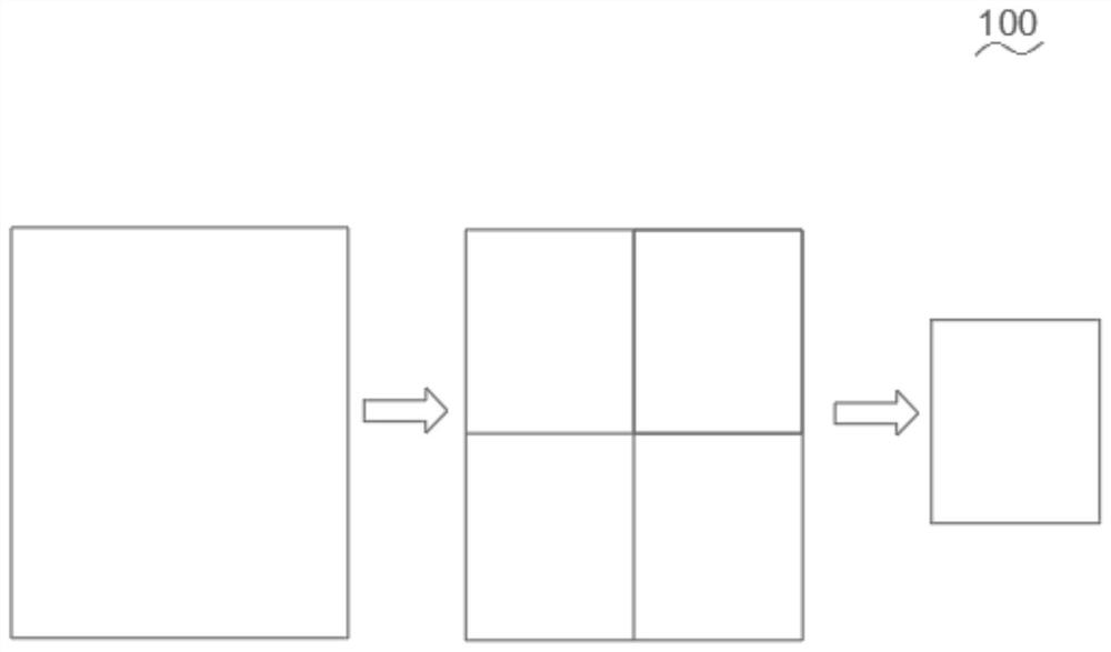
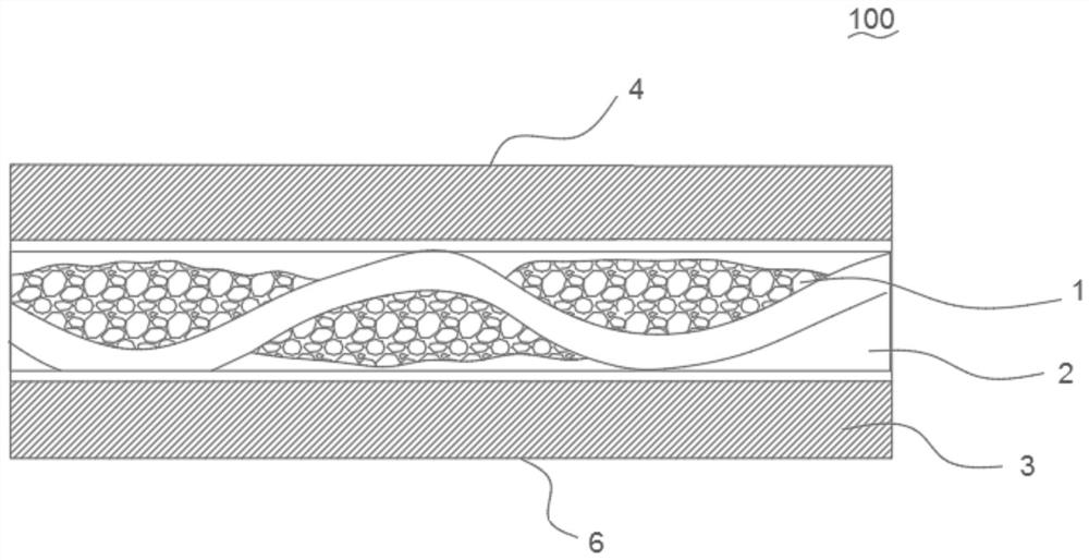
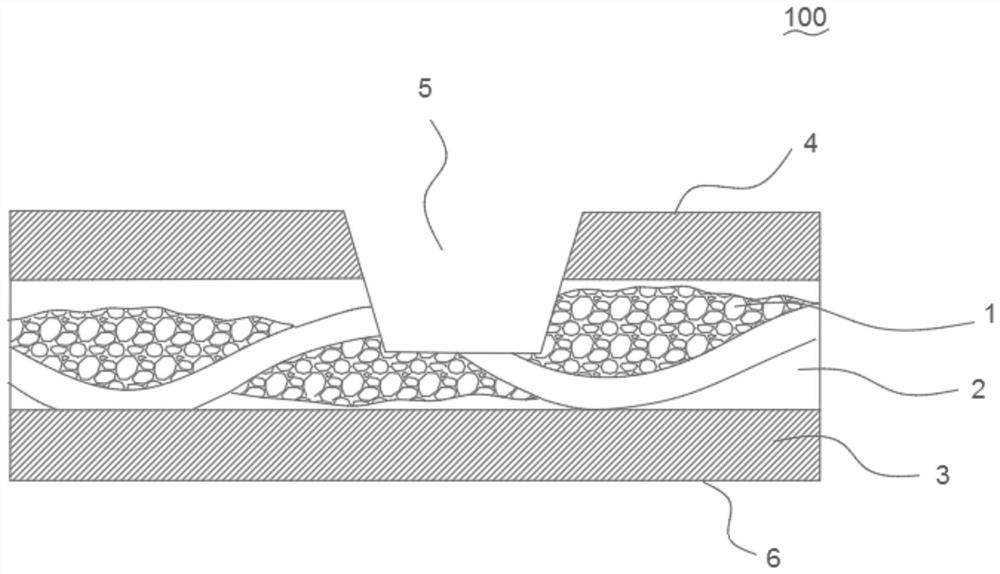
[0041] Such as figure 2 As shown, a circuit board of the present invention includes: a glass fiber cloth 1, a resin 2 is arranged on the glass fiber cloth 1, and the glass fiber cloth 1 and the resin 2 form a base plate, and the base material Metal layers 3 are provided on both sides of the board, and the base board and the metal layer 3 form a core board 100 .

[0042] The core board 100 is provided with an opposite first surface 4 and a second surface 7, please refer to image 3 , Figure 5 , the first surface 4 opens a plurality of first blind holes 5 to the second surface 6, and the second surface 6 opens a plurality of second blind holes 7 to the first ...


PUM


Abstract

The invention provides a manufacturing method of a circuit board, which comprises the following steps of: 1) providing a core board which is provided with a first surface and a second surface which are opposite to each other; 2) forming positioning holes in the core plate; (3) positioning is carried out through the positioning holes, performing laser drilling on the core plate, machining a plurality of first blind holes in the first face, and distributing and drilling the drilling lines of the first blind holes according to a spiral path from outside to inside when the first face is drilled; and (4) turning over the core plate, performing positioning through the positioning holes, machining a plurality of second blind holes in the second face, and when the second blind holes are drilled inthe second face, drilling lines correspondingly drill holes according to a spiral path from outside to inside, so that the first blind holes drilled in the first face and the second blind holes drilled in the corresponding second face are coaxially communicated. The paths for drilling the blind holes in the two surfaces of the core plate are the spiral lines from outside to inside, so that the core plate is deformed into uniform shrinkage, deformation caused by local overheating of the core plate is avoided, and the communication accuracy of each first blind hole and the corresponding secondblind hole is improved.

Description

technical field [0001] The invention relates to the technical field of circuit board manufacturing, in particular to a method for manufacturing circuit board drilling holes. Background technique [0002] With the development trend of light, thin and small electronic products, the demand for multilayer circuit board products is gradually increasing. However, the poor reliability of laser blind holes in the core board and the difficulty in filling and leveling the through holes in the core board, and other technical bottlenecks have become important reasons that limit its development. Therefore, the "X-shaped hole" (laser drilling on both sides of the same hole to form a through hole with some protrusions in the hole) has gradually entered everyone's field of vision, but the problem of misalignment of the laser holes on both sides of the same hole position has become a problem for everyone. problem. [0003] Excluding the deviation of about 10 μm caused by the accuracy of th...

Claims


Application Information

Patent Timeline
Patent Type & Authority Applications(China)
IPC IPC(8): H05K3/00H05K3/40H05K1/11
CPCH05K1/115H05K3/0008H05K3/0047H05K3/4038H05K2203/0221
Inventor 何思良纪成光赵刚俊刘梦茹
Owner DONGGUAN SHENGYI ELECTRONICS
Why Eureka
Try Eureka