Optical proximity correction method for contact hole photoetching process hot spot

A technology for optical proximity correction and photolithography, which is used in optics, photolithography for patterned surfaces, originals for optomechanical processing, etc.

Active Publication Date: 2020-11-13
SHANGHAI HUALI MICROELECTRONICS CORP
View PDF5 Cites 0 Cited by
  • Summary
  • Abstract
  • Description
  • Claims
  • Application Information

AI Technical Summary

Problems solved by technology

The introduction of scattering strips helps to design a better imaging OPC pattern, but there will still be process hotspots in the OPC pattern caused by contact hole edge errors. Therefore, improving the contact hole process hot spots that still exist in the OPC pattern becomes Technical issues that the industry needs to explore

Method used


Image

  • Optical proximity correction method for contact hole photoetching process hot spot
  • Optical proximity correction method for contact hole photoetching process hot spot
  • Optical proximity correction method for contact hole photoetching process hot spot

Examples


Embodiment Construction

[0036] The specific implementation manner of the present invention will be described in more detail below with reference to schematic diagrams. The advantages and features of the present invention will be more apparent from the following description. It should be noted that all the drawings are in a very simplified form and use imprecise scales, and are only used to facilitate and clearly assist the purpose of illustrating the embodiments of the present invention.

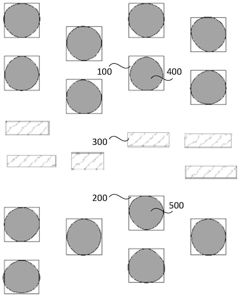
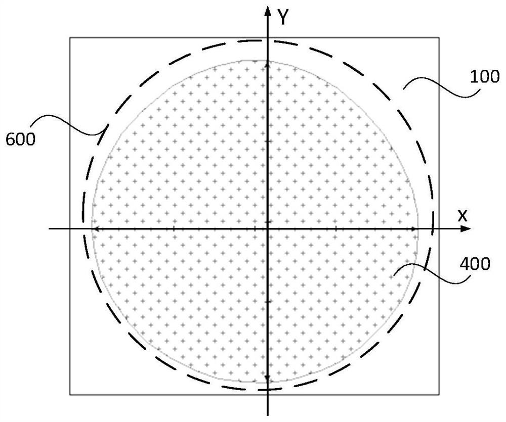
[0037] figure 1 It is a schematic diagram of the OPC graph in this embodiment. Such as figure 1 As shown, the contact hole area in the OPC pattern will have a pattern-dense area and a pattern-sparse area. The light scattering effect of the sparse pattern area is weaker than that of the pattern dense area, resulting in a smaller photolithography process window in the pattern sparse area than in the pattern dense area, which further leads to a smaller overall process window of the OPC pattern. .

[0038] The lit...


PUM

PropertyMeasurementUnit
transmittivityaaaaaaaaaa

Abstract

The invention provides an optical proximity correction method for a contact hole photoetching process hot spot. The method comprises the following steps: providing an OPC pattern which is provided with a contact hole area; adding a sub-resolution auxiliary pattern to a blank area of the contact hole area; and moving the sub-resolution auxiliary pattern step by step to improve the edge error of thecontact hole. According to the optical proximity correction method for a contact hole photoetching process hot spot, through moving the sub-resolution auxiliary graph, the light scattering effect ofthe sub-resolution auxiliary graph on the contact hole area is changed, the light intensity distribution of the contact hole area is further adjusted, the corner contour is enhanced and the exposure focal depth is increased, so that the edge error of the contact hole is improved, and the process hotspot caused by the edge error of the contact hole in the OPC graph is improved.

Description

technical field [0001] The invention relates to the technical field of semiconductor manufacturing, in particular to an optical proximity correction method for a hot spot in a photolithography process of a contact hole. Background technique [0002] As the process nodes of integrated circuit devices continue to shrink, the Optical Proximity Effect (OPE) becomes more and more serious, and the traditional Optical Proximity Correction (OPC) technology can no longer meet the process requirements. As a result, the optical proximity correction technology has evolved into the Sub-Resolution Assist Feature (SRAF), which is widely used in the key-level OPC publishing process below the 55nm technology node. [0003] Usually, in an OPC graphic being designed, there are both pattern-intensive areas and pattern-sparse areas, and the lithography process window of the pattern-sparse area is smaller than that of the pattern-intensive area, which leads to a smaller common process window. . ...

Claims


Application Information

Patent Timeline
Patent Type & Authority Applications(China)
IPC IPC(8): G03F1/36
CPCG03F1/36
Inventor 胡青何大权张辰明魏芳朱骏
Owner SHANGHAI HUALI MICROELECTRONICS CORP
Why Eureka
Try Eureka