Touch panel and preparation method thereof and display device

A touch panel and touch area technology, applied in instruments, semiconductor devices, computing, etc., can solve the problem of high production cost of touch panels

Pending Publication Date: 2020-12-04
BOE TECH GRP CO LTD +1
View PDF0 Cites 10 Cited by
  • Summary
  • Abstract
  • Description
  • Claims
  • Application Information

AI Technical Summary

Problems solved by technology

[0006] The technical problem to be solved in the present disclosure is to provide a touch panel and ...

Method used


Image

  • Touch panel and preparation method thereof and display device
  • Touch panel and preparation method thereof and display device
  • Touch panel and preparation method thereof and display device

Examples


Embodiment approach

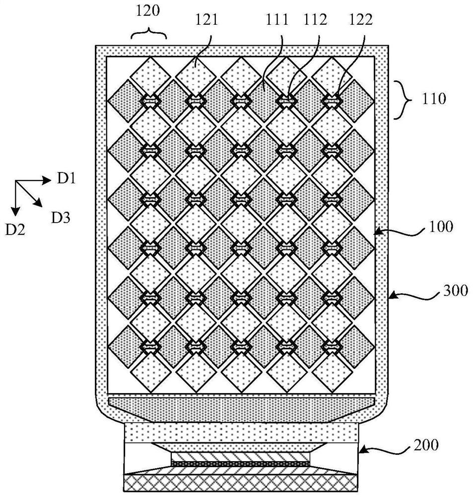
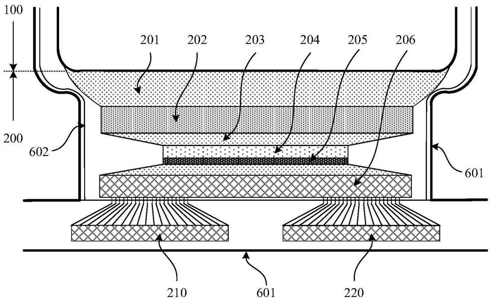
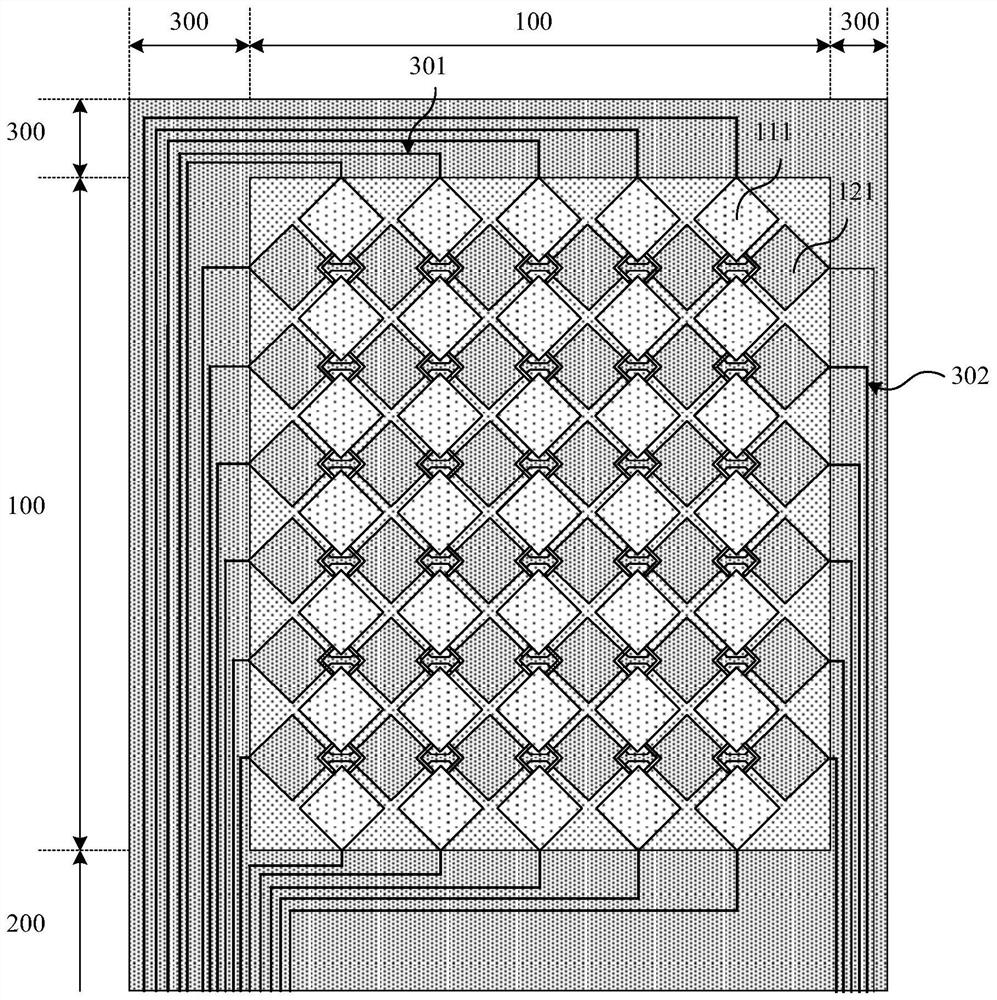
[0207] The present disclosure also provides a method for manufacturing a touch panel. The touch panel includes a display area and a binding area located on one side of the display area. Along the direction away from the touch area, the binding area includes at least The first fan-out area, the bending area, the second fan-out area, the driver chip area and the binding pin area are set; along the direction parallel to the edge of the binding area, the binding pin area includes the The first pin area on the first side of the binding area and the second pin area on the second side of the binding area, the edge of the binding area is the edge of the binding area adjacent to the touch area. In an exemplary embodiment, the preparation method includes:

[0208] A plurality of transfer wires are formed in the second fan-out area of ​​the binding area; or, a plurality of transfer wires are formed in the outer pin bonding area between the driver chip area and the binding pin area;

[0...


PUM


Abstract

The invention discloses a touch panel and a preparation method thereof and a display device. The touch panel comprises a touch area, a binding area located on one side of the touch area and an edge area located on the other side of the touch area. The touch area at least comprises M rows of first touch units and N columns of second touch units, the binding area at least comprises a binding pin area, and the edge area at least comprises a plurality of touch leads; and the first ends of the plurality of touch leads are respectively and correspondingly connected with the M rows of first touch units and the N columns of second touch units, and the second ends of the plurality of touch leads extend to the binding area and are correspondingly connected with the plurality of pins of the binding pin area, wherein M and N are positive integers greater than 2. According to the invention, the implementation cost and the production cost are effectively reduced.

Description

technical field [0001] The present disclosure relates to but not limited to the field of display technology, especially a touch panel, a manufacturing method thereof, and a display device. Background technique [0002] With the rapid development of display technology, touch screens (Touch Screen) have gradually spread in people's lives. According to the structure, the touch screen can be divided into add-on mode (Add on Mode), surface-covering type (On Cell), embedded type (InCell), etc. According to the working principle, the touch screen can be divided into capacitive, resistive, infrared, surface acoustic wave and so on. The capacitive On Cell type is a touch structure formed on the surface of the light-emitting side of the display. Due to its advantages of simple structure, thin thickness, and high transmittance, it has gradually become the mainstream technology. [0003] Organic Light Emitting Diode (OLED) is an active light-emitting display device, which has the adva...

Claims


Application Information

Patent Timeline
IPC IPC(8): G06F3/041G06F3/044H01L27/32
CPCG06F3/0412G06F3/0444G06F2203/04103H10K59/00G06F2203/04107G06F3/04164G06F3/0446G06F2203/04111
Inventor 韩林宏刘庭良张毅牛文骁秦世开高永益
Owner BOE TECH GRP CO LTD
Why Eureka
Try Eureka