
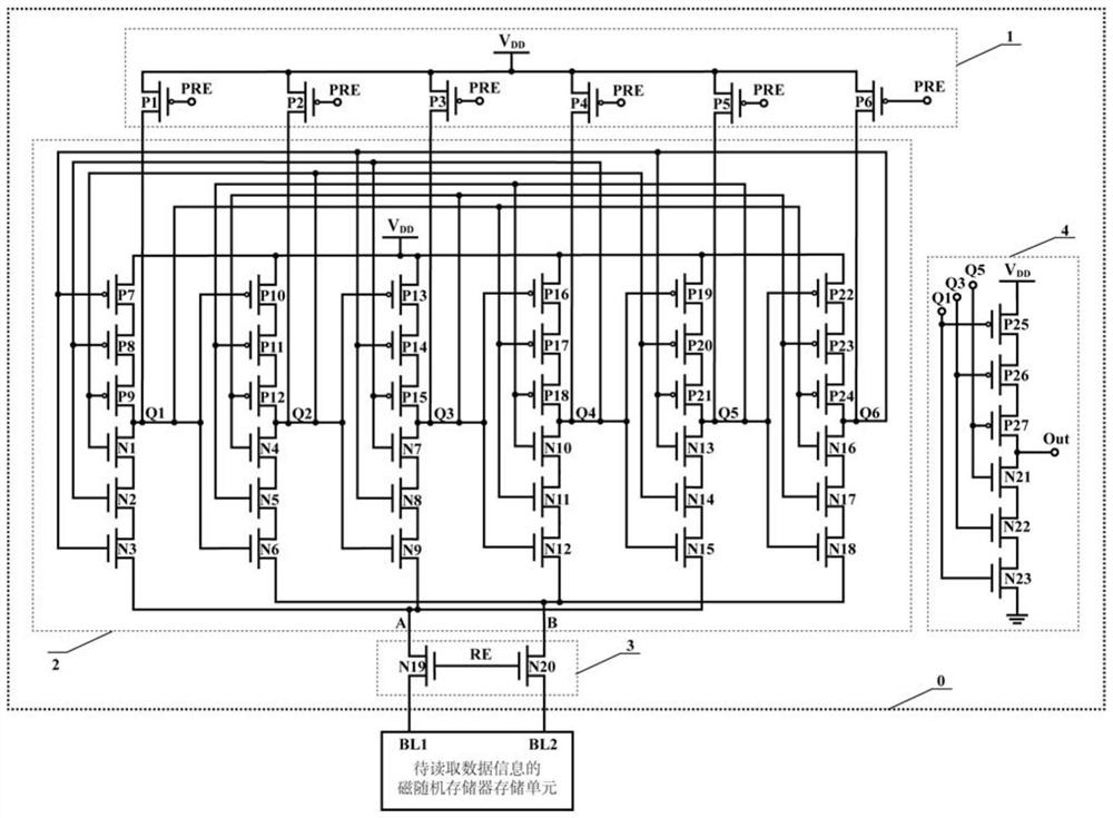
Magnetic memory reading circuit capable of resisting single-event double-node upset based on C unit

A dual-node flip, anti-single particle technology, applied in static memory, digital memory information, information storage and other directions, can solve problems such as unreliable data reading

Active Publication Date: 2020-12-08
HEFEI INNOVATION RES INST BEIHANG UNIV
View PDF10 Cites 1 Cited by
  • Summary
  • Abstract
  • Description
  • Claims
  • Application Information

AI Technical Summary

Problems solved by technology

[0003] The present invention aims at the above-mentioned problem of unreliable data reading due to double-node flipping of the differential signal reading circuit, which cannot be solved by the existing technical solutions for anti-single-event flipping

Method used


Image

  • Magnetic memory reading circuit capable of resisting single-event double-node upset based on C unit
  • Magnetic memory reading circuit capable of resisting single-event double-node upset based on C unit
  • Magnetic memory reading circuit capable of resisting single-event double-node upset based on C unit

Examples


Embodiment Construction

[0057] In order to make the purpose, technical solutions and advantages of the embodiments of the present invention clearer, the technical solutions in the embodiments of the present invention will be clearly and completely described below in conjunction with the drawings in the embodiments of the present invention. Obviously, the described embodiments It is a part of embodiments of the present invention, but not all embodiments.

[0058] A magnetic memory read circuit based on the C unit anti-single event dual-node flip in the embodiment of the present invention can not only realize the data information reading function with fast speed and low power consumption, but also has anti-single event during the data information reading process. The ability to flip over two nodes. The substantive features of the present invention will be further described below according to the accompanying drawings and specific implementation examples.

[0059] A magnetic tunnel junction (Magnetic T...


PUM


Abstract

The invention relates to a magnetic memory reading circuit capable of resisting a single-event double-node upset based on a C unit. The magnetic memory reading circuit is characterized in that the input end of a pre-charging circuit is connected with a pre-charging signal PRE; the output end of the pre-charging circuit is connected with an internal node Q1, an internal node Q2, an internal node Q3, an internal node Q4, an internal node Q5 and an internal node Q6 of a latch circuit; the output end of the latch circuit is connected with the input end of a read circuit separation module. the output end of the read circuit separation module is connected with a bit line BL1 and a bit line BL2 of a magnetic random access memory storage unit having data information to be read; the input end of anoutput circuit is connected with the internal node Q1, the internal node Q3 and the internal node Q5 of a latch circuit module; and the output end OUT of an output circuit module is the output end ofthe magnetic memory reading circuit . According to the magnetic memory reading circuit, not only can a data information reading function be realized at high speed and low power consumption, but alsothe single-event double-node upset resistance is realized in the data information reading process.

Description

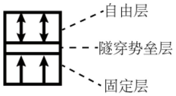
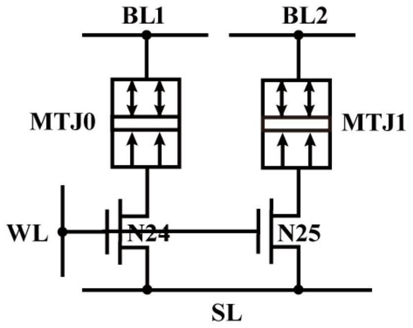
technical field [0001] The invention relates to the field of anti-radiation hardening of integrated circuits and non-volatile storage intersecting technologies, in particular to a magnetic memory read circuit based on C unit anti-single-event double-node flipping. Background technique [0002] Magnetic random access memory (Magnetic Rand om Access Memory, MRAM) has great application potential in the aerospace field in the future due to its non-volatile, low power consumption, fast access, inherent radiation resistance and other characteristics. MRAM is mainly composed of a memory cell array and peripheral read and write circuits. As a memory unit of MRAM, a magnetic tunnel junction (Magnetic Tunnel Junction, MTJ) is mainly composed of two ferromagnetic layers and a tunneling barrier layer sandwiched between them. One of the ferromagnetic layers has a fixed magnetization direction and is called a pinned layer; while the other ferromagnetic layer has a variable magnetization ...

Claims


Application Information

Patent Timeline
IPC IPC(8): G11C11/16
CPCG11C11/1673G11C11/161G11C11/1697
Inventor 张德明王贤张凯丽赵巍胜
Owner HEFEI INNOVATION RES INST BEIHANG UNIV
Learn More